A great deal has been written of late about the demise of Moore’s Law. The increase in field-effect transistor density with successive process nodes has slowed from the 2X every 2 1/2 years pace of earlier generations. The economic nature of Moore’s comments 50 years ago has also been scrutinized – the reduction in cost per transistor has also abated.
The traditional technology scaling model has become significantly more complex, due to the requirements for: new lithography systems and resists; alternative deposition and etch equipment; the introduction of new interconnect and dielectric materials; and, the increasingly reliance on new design-technology co-optimization (DTCO) integration methods.
Parenthetically, the emergence of various 2.5D and 3D multi-die packaging offerings has led to the use of the term “More than Moore” integration. The potential diversity of die functionality and process selection in these packages offers additional tradeoffs in realizing effective density and cost, the foundations of Moore’s Law.
Despite all of the commentary on Moore’s Law, there remains a tremendous R&D investment on new devices that will continue to offer improved performance, power, and area. At the recent Advanced Semiconductor Manufacturing Conference (ASMC), sponsored by SEMI, a highlight was the keynote presentation by Gary Patton, CVP & GM, Design Enablement, at Intel, who presented an overview of these R&D efforts. His “Continuing Moore’s Law” talk offered an optimistic view on future technology features.
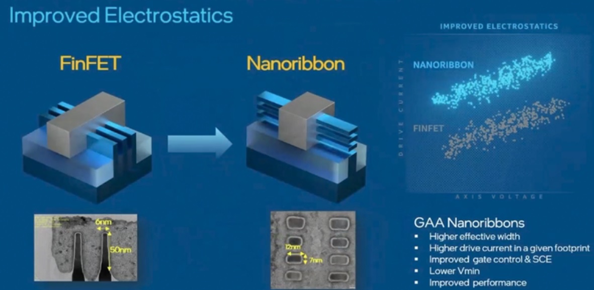
Gary covered the transition to gate-all-around (GAA) devices, expected to be the immediate successor to FinFETs. (With the re-introduction of devices where the individual transistor width is again a design parameter, the transistors/mm**2 density measure will likely need a re-interpretation.)
There are numerous research initiatives underway as a potential long-term transition beyond CMOS – e.g., (arrays of) 2D semiconductor materials, such as MoS2, WS2, and WSe2.
Of particular note in Gary’s talk was the description of an area of process technology development that perhaps does not receive due consideration – the 3D monolithic integration of heterogeneous semiconductor materials, used for fabrication of optimized nFET and pFET devices. This approach provides continued device scaling, integration of mature process fabrication techniques, and builds upon existing (CMOS-based) circuit design experience.
Before elaborating on some of the monolithic 3D possibilities, a description of the bonding of heterogeneous materials would be insightful.
Oxide Bonding and Donor Wafer Cleaving
The goal of monolithic 3D integration is to provide multiple, stacked semiconducting materials for device fabrication. A subset of transistors is fabricated in the host wafer. Subsequently, a donor wafer (of a different semiconductor composition) is bonded to the host, and cleaved to provide a thin material layer on top of the host for subsequent device processing. The figures below illustrate the wafer process flow.
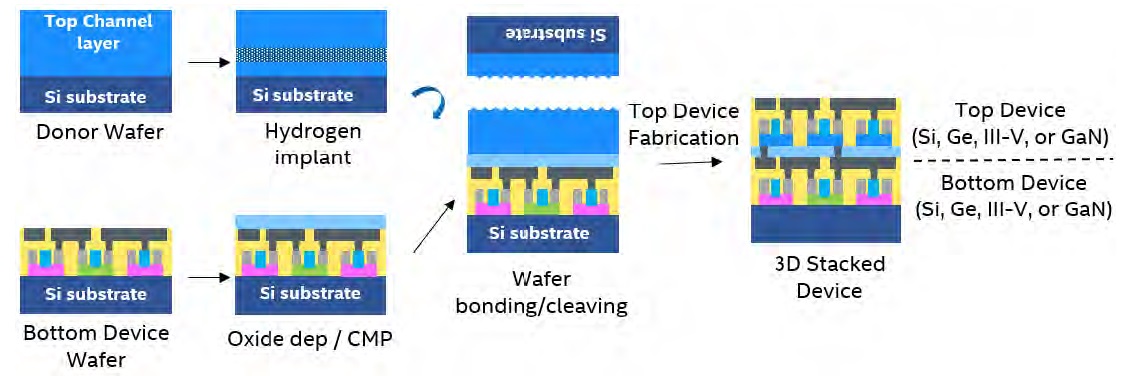
The full-thickness host wafer provides the mechanical support; the thin donor layer does not add significantly to the overall thickness, enabling the use of existing process equipment and fabrication flows. (As will be discussed shortly, there are restrictions on the thermal budget for processing the donor layer devices, so as not to adversely impact the existing host device characteristics.)
Briefly, the sequence of steps for preparation of the 3D monolithic stack is:
- devices are fabricated on the host (300mm) wafer
- the host wafer receives a deposition of a thin dielectric layer (e.g., chemical vapor deposition of SiN and SiO2)
- the host wafer surface is polished (e.g., using chemical-mechanical polishing)
- a (300mm) donor wafer is subjected to an implant of H+ (protons), using an optimized implant energy and dose
- the donor and host wafers are bonded
Prior to bonding the host and donor wafers, specific wafer surface cleaning chemistries are employed. It is necessary that the two wafer surfaces are hydrophilic, “atomically smooth”, and have a high density of chemical bonding sites (to preclude micro-voids forming at the interface).
In a special aligner (with dual wafer chucks), the host and donor wafers are loaded facing each other, aligned, and brought in contact. After the initial wafer-to-wafer interface bonding has stabilized, the donor chuck is released.
Then, a thermal annealing step is applied to the composite. This anneal performs two critical functions: it strengthens the bonded interface, and it allows the implanted hydrogen to diffuse in the semiconductor crystal, and nucleate to form H2.
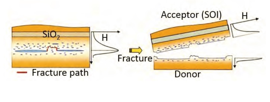
A very thin H2 layer forms in the donor wafer, at a depth equivalent to the point of highest crystalline dislocation after the H+ implant. This H2 layer introduces a structurally weak interface within the donor wafer crystal.
- the donor wafer is cleaved at the internal H2 interface
A combination of mechanical edge force and/or thermal cycling results in fracturing of the donor wafer at the H2 layer depth.
- the resulting monolithic wafer with the stacked sequence of semiconductor layers is annealed (to reduce residual implant damage), and polished
As illustrated above, the fracturing step may result in a rough surface topography, which needs to be polished before subsequent device fabrication, and layer-to-layer contact formation.
This technique for oxide bonding and donor layer transfer has been used in production for silicon-on-insulator (SOI) wafer preparation for many years. (A deeper understanding of the mechanics behind H+ diffusion, H2 layer formation, and the structural impact on the donor wafer crystal during the nucleation annealing step remains an active area of research.)
Gary’s presentation highlighted two areas where the Intel Research division is adapting this layer transfer technique to 3D monolithic integration, to further extend Moore’s Law.
nFET in Si, pFET in Ge
One of the issues faced in advanced process development is the relatively weak hole mobility in Si, especially at higher hole free carrier density and electric field. Current process technologies incorporated compressive mechanical stress in the pFET device channel to improve the hole mobility. More recent advances strive to utilize a stoichiometric combination of Si and Ge directly in the pFET device channel – i.e., Si(x)Ge(1-x) – to leverage the higher hole mobility in Ge.
The team at Intel Research has been pursuing 3D monolithic integration using a Ge donor layer bonded on top of the Si host wafer, as depicted below. [1]
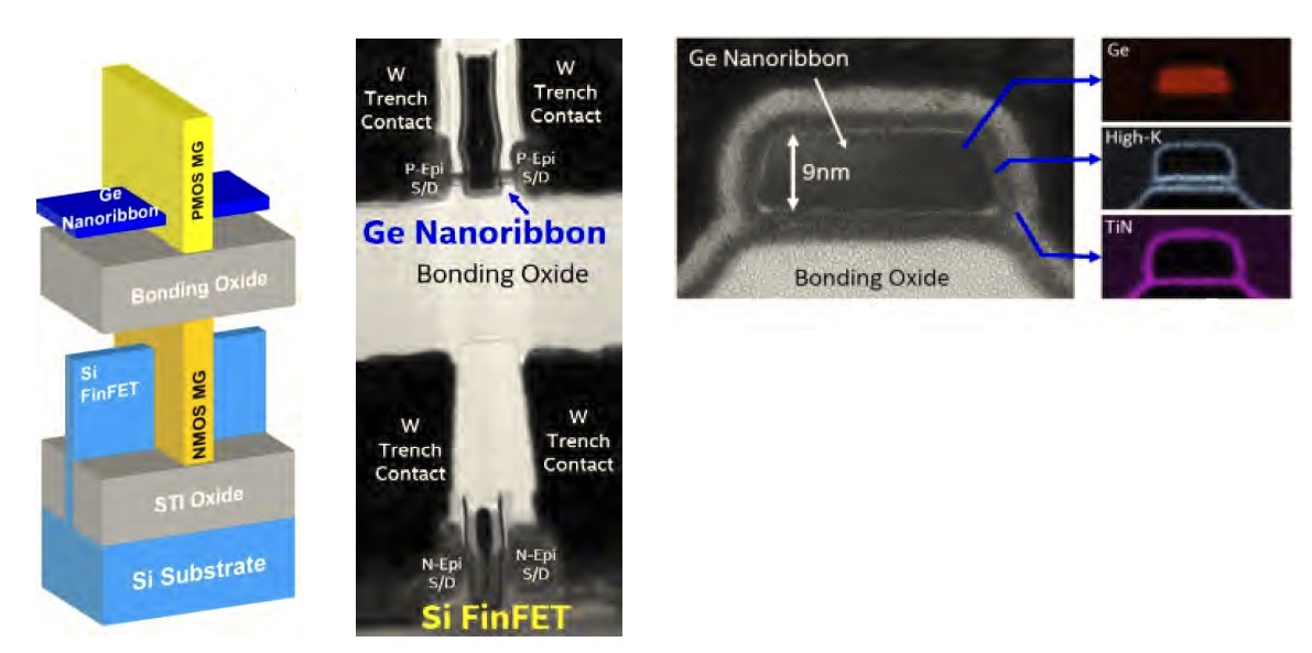
In this case, a FinFET device structure was fabricated on the host wafer for the nFETs, while a GAA topology was used for the pFETs in the Ge donor layer. As mentioned above, the process flow and materials selection for the nFET high-K, metal gate, source/drain doped epitaxy, and contact metal is chosen to be compatible with the subsequent thermal processing of the Ge donor layer and pFET fabrication (e.g., <600C).
After the fabrication of the GAA pFET source/drain epi, device oxide and metal gate (using a replacement gate process), and source/drain contacts, vias are formed between the two transistor layers.
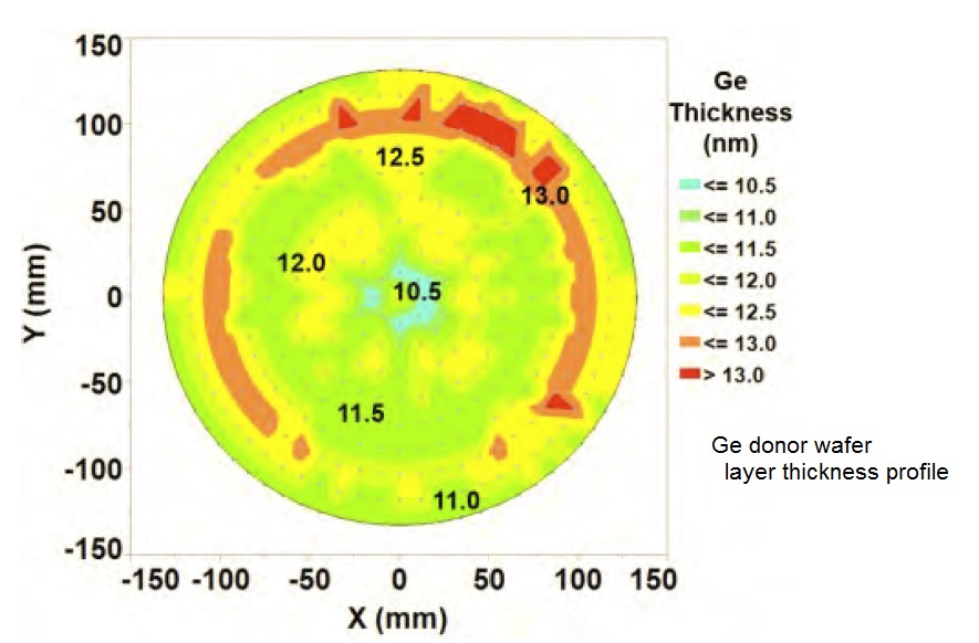
Also illustrated above is an example profile of the Ge donor layer thickness across a 300mm wafer, showing excellent uniformity of the monolithic layer transfer process (<3nm variation across the entire wafer).
The figures below depict the final 3D cross-section, the (short-channel) Si nFET and Ge pFET characteristics, and the Vout versus Vin transfer characteristics of a 3D monolithic inverter logic gate (down to VCC = 0.5V). The Ion versus Ioff curve for the Ge pFET illustrates the improved characteristics over strained Si devices.
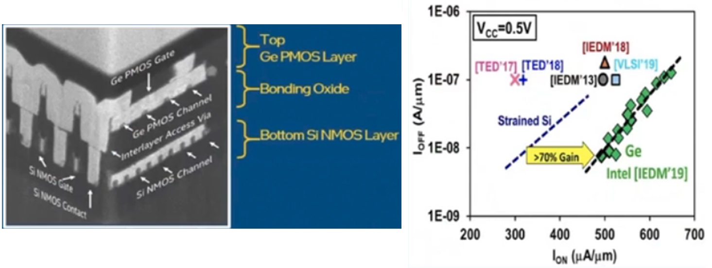

The use of a Ge layer stacked vertically on top of a Si layer for heterogeneous integration offers a unique opportunity for CMOS logic implementations, helping to extend Moore’s Law.
Si donor wafer on GaN host
The previous section described an approach to realize improved hole mobility in Ge pFETs. Another area where advanced process development issues have arisen is the need for high-efficiency RF-class devices, integrated with conventional CMOS logic. The demand for 5G (and beyond) applications requires optimum device cutoff frequency (Ft) and maximum oscillation frequency (Fmax) response, for mmWave power amplifiers, with corresponding low noise characteristics for low-noise amplifiers, and with fast switching speed for RF switches. The excellent Ioff and low Ron of the enhancement-mode GaN device is attractive for high-efficiency integrated voltage regulator designs, as well.
Gary highlighted the work done by the Intel Research team to develop monolithic heterogeneous integration of GaN devices with conventional Si CMOS circuitry. [2]
The figures below illustrate the fabrication of a variety of GaN components, fabricated in an epitaxial layer on the host wafer (a Si substrate) – e.g., enhancement-mode and depletion-mode nFETs, Schottky gate FETs, and Schottky diodes (without the high-k gate oxide dielectric). A cross-section of the final structured is also shown.
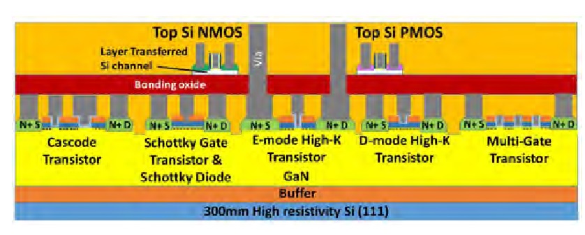
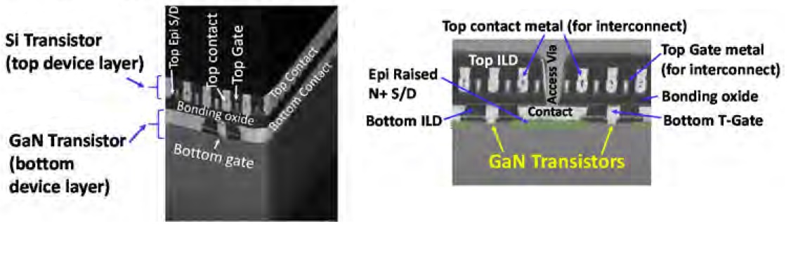
In this case, the donor wafer is Si, used for fabricating nFET and pFET devices, as would be used for analog functions, digital signal processing, and logic/memory. (P-channel GaN devices are extremely challenging to fabricate.)
Whereas the circuit-level CMOS integration of the previous Si nFET and Ge pFET monolithic integration necessitates consistent (and aggressive) design rules, the distinct applications for the (RF) GaN devices and (CMOS) Si devices decouples the two technologies. The GaN devices can be much different in dimension than the FETs – e.g., W > 10um for very low Ron – or with much longer channel lengths supporting high-voltage applications, compared to the Si FinFETs.
As with the host Si nFETs fabricated prior to bonding the donor Ge pFET layer, the GaN devices much tolerate the thermal budget of the subsequent donor Si layer transfer and nFET/pFET device fabrication.
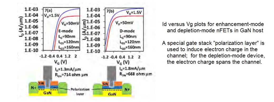
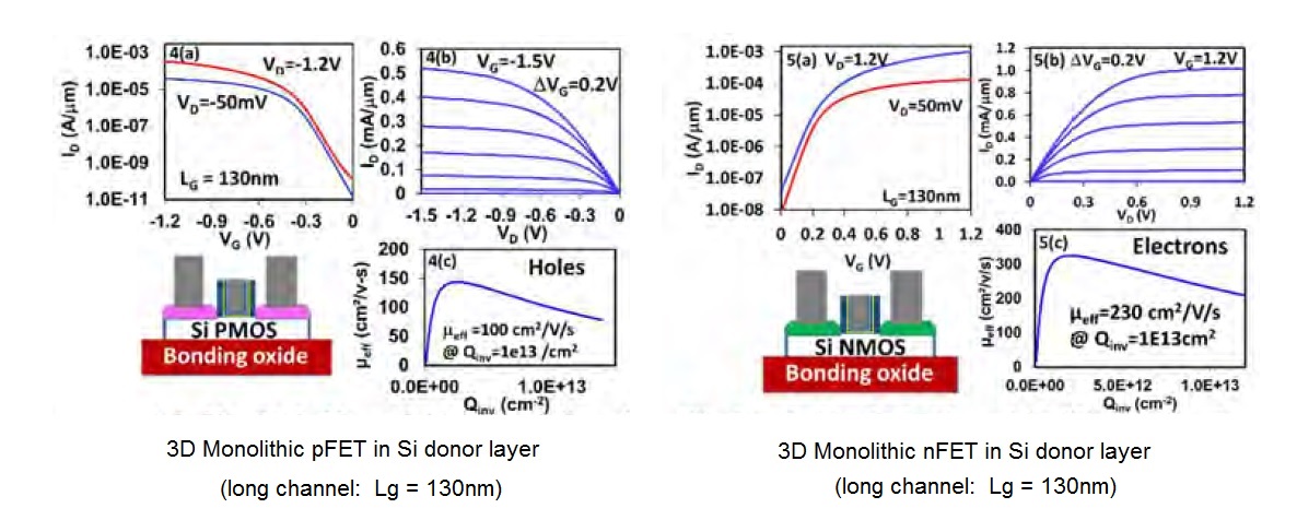
Representative Ids versus Vg curves for the (long-channel) GaN enhancement-mode and depletion-mode nFET devices are shown below, along with the Si nFET and Si pFET device characteristics fabricated in the donor layer.
Summary
The next evolution in Moore’s Law from FinFET devices will be GAA topologies. The opportunity to continue Moore’s Law may indeed be facilitated by 3D monolithic integration, extending the bonded layer transfer technology used for SOI wafer fabrication to a wider variety of semiconducting materials, such as Ge and GaN. This will help alleviate the risks associated with the introduction of “beyond CMOS” materials processing.
It will be extremely interesting to track the progress and innovations in vertical stacking of devices of various types, for applications ranging from high-performance computation to high-frequency RF signal processing.
Epilogue
A passing comment at the ASMC from a member of the academic community caught my attention. He said, “I’m seeing a diminished interest among students in pursuing microelectronics as an area of study. They hear that ‘Moore’s Law is dead’, and conclude the field has stagnated.”
Frankly, I cannot recall a time when there have been more opportunities for major advances in device research, processing technology, and circuit/systems applications development than at present. If you are a student reading this article, please realize that there are many exciting careers ahead in extending Moore’s Law.
-chipguy
References
[1] Rachmady, W., et al., “300mm Heterogeneous 3D Integration of Record Performance Layer Transfer Germanium PMOS with Silicon NMOS for Low Power High Performance Logic Applications”, IEDM, 2019, p. 29.7.1 – 29.7.4.
[2] Then, Han Wui, et al., “GaN and Si Transistors on 300mm Si(111) enabled by 3D Monolithic Heterogeneous Integration”, 2020 VLSI Symposium, paper THL.2.
Share this post via:


Comments
There are no comments yet.
You must register or log in to view/post comments.