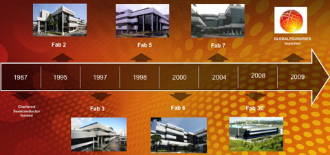
GlobalFoundries has been in Singapore for a long time. Longer than GlobalFoundries has existed in fact. Chartered Semiconductor was started in Singapore in 1987 and GF acquired them in early 2010 less than a year after they were created by spinning out the manufacturing arm of AMD. When GF was started their state of the art fab was in Dresden (Germany) and their new state of the art fab is in New York state. GlobalFoundries is committed to Singapore and is expanding there, investing $500M under the umbrella title Singapore Vision 2015. In the paragraph above I talked about state of the art fabs, but you have to look at the end application too. For power ICs, 180nm is the state of the art process. It is also a big market. The market for analog and power ICs manufactured on mature processes is $45B and is growing at 15% CAGR, faster than the overall semiconductor market. The market is changing too. Most of these specialized chips were manufactured by specialized IDMs, but these designs have moved to process generations beyond what most specialized IDMs have in-house, and so naturally have also migrated to the foundry model just as high complexity SoCs did over the last couple of decades. This is not driven by the latest SoC for your smartphone (those other two fabs are for that) but by all the analog/mixed-signal which is everywhere. In your smartphone for a start…  In fact, if you tear down a typical smartphone you’ll find four digital chips (the application processor, the baseband processor (these may be combined) and flash memory. But there are 8 analog chips for everything from power management, display drivers, gyroscopes and so on. But there is also a big analog mixed signal component in storage, automotive, industrial, mil/aero.
  There are currently 6 GlobalFoundries’ fabs in Singapore (numbered 2, 3, 5, 6, 7 and 3E). The oldest, fab 2, was opened in 1995. The most recent, 3E, in 2008.
  So what are they doing with that half billion dollar investment?
- Refreshing the 200mm assets
- Expanding the 300mm fab 7 giving the benefits of modular process flexibility with 300mm efficiency and scalability
- Fab 6 will also be converted from 200mm to 300mm
- That will take Singapore to around 1M 300mm wafers per year (2.6M 8″ equivalents, the “standard” measure) 2/3 of capacity up from 1/3 today
- Aligning product and manufacturing portfolio in line with target markets with a focus on advanced analog, non-volatile memory, digital, power and RF
- Reducing manufacturing complexity and increasing manufacturing scalability through a modular technology platform.
Read more about Vision 2015 and Foundry 2.0 here. 


Musk’s Orbital Compute Vision: TERAFAB and the End of the Terrestrial Data Center