In the 1980s, Japan was seen as the leader in the semiconductor industry. Their quality was higher, especially in memories, and the US was worried about falling behind. In fact Sematech was created in 1987 by the US government and a consortium of 14 US-based semiconductor companies primarily to pool investment on common problems and regain competitiveness of the US semiconductor industry versus the Japanese. However, today, Japan is largely seen as an also-ran in the semiconductor business. It is very inwardly focused on the Japanese market, and consolidation really is only allowed to happen in Japan, so that Hitachi and Mitsubishi merged to form Renasas and the NEC’s semiconductor business was folded in too and then bailed out by the Japanse government. Meanwhile, Elpida became the focus for memory but eventually filed for bankruptcy and is (probably) being acquired by US-based Micron.
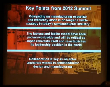
Earlier this month at the Nikkei Electronics’ World Semiconductor Industry Summit in Tokyo, Global Foundries’ CEO Ajit Manocha presented “Reshaping the Foundry Industry: Welcome to Foundry 2.0” where he outlined the evolution of the foundry model and, in particular, what it will take for Japanese IDM companies to regain their former glory. In particular, he urged them to embrace the fabless/fablite model rather than continuing to invest in their own process technology development and their own manufacturing. Today, just 5% of the volume manufactured by foundries comes from Japan.
The challenge is huge. Japan no longer has leading edge capacity (20nm and below) and although there are 42 new fabs under construction worldwide in 2011-13, not one of them is in Japan (or owned by a Japanese semiconductor company). Mobile is an area where Japan has been especially inwardly focused, with their own standards. In many ways the Japanese mobile market is the most advanced in the world, but the suppliers compete aggressively inside Japan while they have largely (with the exception of Sony) given up on the global market.
What Ajit calls Foundry 2.0 is a collaborative virtual-IDM. The old foundry model will no longer work due to the complexity of the process and the accelerated adoption ramp. Instead the responsibilities need to be more cooperative, with the foundry taking the lead for technology architecture, PDKs, manufacturing etc, and the semiconductor company taking responsibility for system architecture, SoC design, IP, final test. But all these need to be developed in parallel so that when the process is ready, the SoCs (especially for mobile) are ready and the volume can ramp very fast.
A video of Ajit’s presentation is here (45 minutes).
Share this post via:


Silicon Insurance: Why eFPGA is Cheaper Than a Respin — and Why It Matters in the Intel 18A Era