I made it through the Virtual Intel Architecture Day last week and much to my surprise it was very well done. Virtual events have been hit and miss but this one was definitely a hit. Great content, approachable experts, a glitch-free experience. The mainstream media has been redundantly covering it so let me add my many years of experience, observation, and opinion because that is what a real semiconductor blogger does, absolutely.
I have asked Scott Jones and Tom Dillinger to blog it as well.

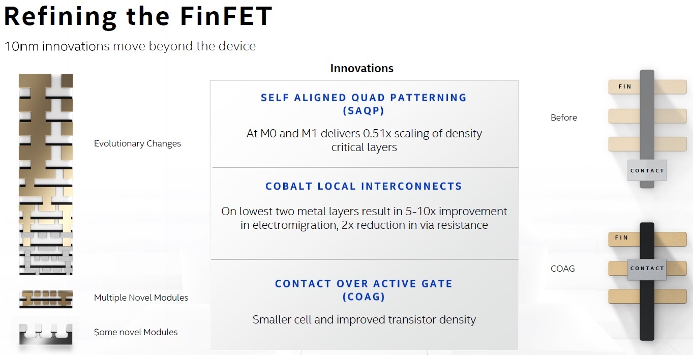
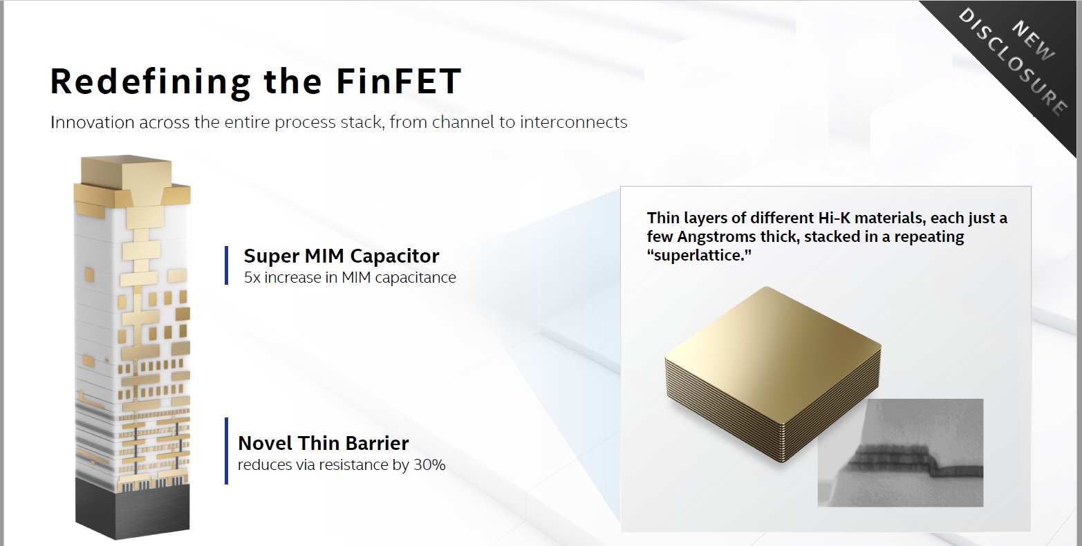
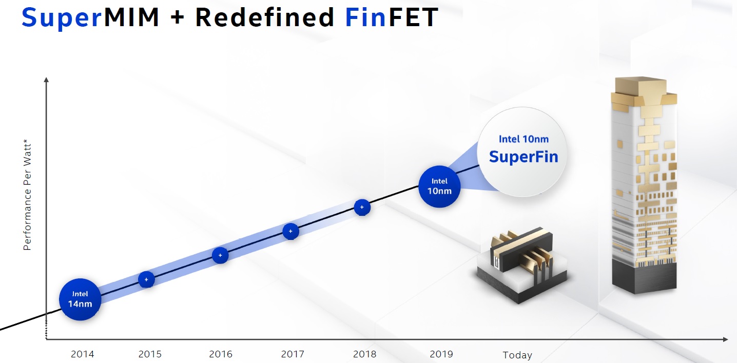
Intel announced the NEW 10nm SuperFin technology with NEW SuperMIM capacitors. I warned Intel about making up semiconductor technology words back when they introduced 22nm and called it TriGate technology versus the industry standard FinFET. As history has shown, if you don’t play nice in the ecosystem the ecosystem will not play nice with you.
Tom Dillinger did a more technical blog on SuperFins here:
A “Super” Technology Mid-life Kicker for Intel

The SuperFin technology is replacing the Intel ++++ process naming and is billed as a full process node transition. While I do applaud Intel for getting rid of the ++++ process naming, switching to made up technology names is not the answer.

One of the best process node naming lessons was when TSMC first came out with FinFETs. The Intel 14nm process was more dense than TSMC’s so out of respect for Intel TSMC went with 16nm. Samsung chose 14nm even though their density was comparable to TSMCs. The end result was TSMC having to explain to customers why their 16nm process was actually better than Samsung’s 14nm. TSMC and Samsung are now in lock step on process node naming with 10nm, 7nm, 5nm, 4nm, and 3nm with comparable densities. Intel could save themselves a lot of time and trouble by playing nice in the ecosystem and following this new industry standard naming.
“Intel’s recent announcement of a delay to its 7nm node sent shockwaves through the tech industry…” NOT!
Another experience, observation, and opinion I have is about the 7nm process delay. Let me make this perfectly clear, process delays for IDMs are very common in the semiconductor industry and Intel is no different. Intel 14nm was delayed, Intel 10nm was delayed, so what is the big surprise with 7nm being delayed? Samsung is in the same boat. In fact, one of the reason’s why Apple left Samsung for TSMC was process delays (Samsung 28nm was VERY late so Apple jumped to TSMC for 20nm). Samsung 10nm, 7nm, and 5nm also experienced high volume production delays. Anybody with a modicum of semiconductor experience knows this to be true.
TSMC also experienced process delays before Apple came along. Anybody here remember 1.3m? How about 40nm? Today TSMC does the Apple two-step delivering new processes every year without fail for the annual iProduct Fall rollout.
And don’t even get me started with the whole “Intel going Fabless” headlines. If anything, the Intel Architecture Day made one thing perfectly clear: Intel will be making their own CPUs until the end of time, absolutely. There is hardly a doubt that Intel placed an order for TSMC wafers because Intel has always been a big customer of TSMC through acquisitions. In fact, most if not all, of the chip acquisitions Intel has made have been TSMC customers. Some of the chips move to Intel manufacturing but some do not. For example, low cost and low power chips (Mobileye) will probably stay at TSMC, my opinion.
Intel DID however announce that they are manufacturing a gaming focused GPU outside of Intel fabs (for the first time) to compete directly with AMD and NVIDIA. Intel did not say which outside fab they are using but since Intel is already a TSMC customer that is a pretty big clue. Also, AMD and NVIDIA both use TSMC so it would be an unnecessary risk for Intel to use yield challenged Samsung. Mystery solved!
Share this post via:


Comments
2 Replies to “Intel 10nm SuperFin Technology!”
You must register or log in to view/post comments.