The outsourcing fabrication of ICs makes them vulnerable to hardware security threats. Security threats such as reverse engineering, insertion of hardware Trojan, and backside contact-less probing to steal cryptographic information can cause financial loss to IP owners and security risk to the system in which these ICs are deployed.
Physical inspection techniques have become more advanced to debug the sub-7 nm advanced technology nodes System on Chip (SoC) or the Heterogeneous Integration (HI) Packaging for failure analysis. However, these advanced inspection techniques developed for debugging can also be used maliciously by an adversary to uncover intellectual property, keys, and memory content.
Previous research has demonstrated that these physical inspection techniques have capabilities as invasive, non- invasive, and semi-invasive to perform hardware-level attacks such as reverse engineering, probing, or circuit editing a chip with the intent to change or decipher the content of the chip. These physical inspection techniques typically perform the attack by scanning and reconstructing netlists or manipulating the chip circuitry.
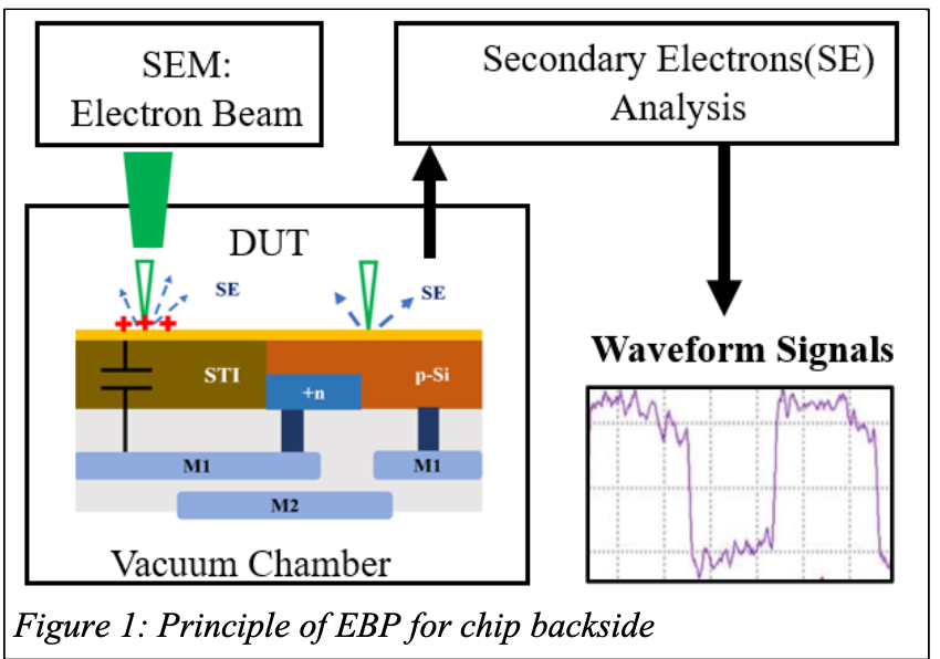
Electron-beam probing (EBP) has emerged as a powerful method as shown in Figure 1, offering 20x better spatial resolution than optical probing, and applies to sub- 7nm flip-chips and advanced 3D architecture systems. In this work, two semi-invasive physical inspection methods: optical probing and E-beam probing, will be discussed and compared in their capabilities in sub-7nm technology nodes for failure analysis and hardware assurance.

Nowadays, EBP takes advantage of the improved beam resolution of modern SEMs resulting in analysis on FinFETs with nm resolution allowing for scaling up into future process generations. The results show that the sample preparation process of EBP, such as bulk silicon removal and shallow trench isolation (STI) exposure has little influence on circuit performance, which makes EBP suitable for semiconductor failure analysis and isolation. Logic states can be read from both memory cell devices and metal lines.
Researchers have successfully performed EBP on active transistors with advanced technology nodes. However, adversaries can take advantage of EBP to attack the sub-7nm technologies devices by extracting valuable information. An adversary will only need traditional failure analysis de-processing tools and an SEM with electrical feed-throughs to prepare and complete unauthorized data extraction in less than a few days. Given its positive results, there is no doubt that the E-beam approach has proven to be the much-awaited need of the industry, and it can continue to inspire ambitious goals, such as achieving a footprint as small as 1 nm. With that said, this paper will serve faithfully to answer the most fundamental questions regarding every aspect of EBP and aid in paving the future roadmap of the semiconductor inspection trade.
With the motivation of lower technology nodes inspection, this paper aims to highlight the importance and need of EBP, mainly focusing on nodes at 7 nm and even below. The focus is on clarifying how all conventional techniques prominent in the IC
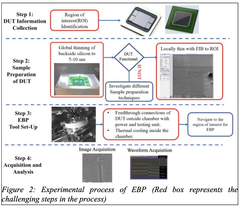
segment physical inspection used to date, including the optical inspection, fail to meet the expectations of the required resolution at the lower nanometer aspirations. Furthermore, backside EBP offers all the advantages frontside EBP did in the 90s: fast signal acquisition, linear VDD signal scaling, and superior signal-to-noise ratio. Our work delves into the principles behind EBP, its capabilities, challenges for this technique as shown in Figure 2, and potential applications in failure analysis and potential attacks. It highlights the need for developing effective countermeasures to protect sensitive information on advanced node technologies. Therefore, Effective countermeasures must be devised to protect sensitive information on advanced node technologies.

Credits:
Navid Asadizanjani
Associate Professor, Alan Hastings Faculty Fellow, Director, Security and Assurance lab (virtual walk), Associate director, FSI, MEST, Department of Electrical and Computer Engineering, Department of Material Science and Engineering, University of Florida
Nitin Vershney
Research Engineer, Florida Institute for Cybersecurity Research
Also Read:
Navigating Frontier Technology Trends in 2024
PQShield Builds the First-Ever Post-Quantum Cryptography Chip
Facing challenges of implementing Post-Quantum Cryptography
Share this post via:


Chemical Origins of Environmental Modifications to MOR Lithographic Chemistry