As your SoC design can contain hundreds of IP blocks, how do you verify that all of the IP blocks will still work together correctly once assembled? Well, you could run lots of functional verification at the full-chip level and hope for the best in terms of code coverage and expected behavior. You could buy an expensive emulator to … Read More
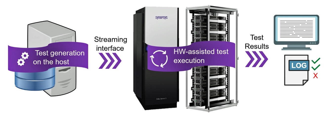 When Software Outruns Silicon: Hardware-Assisted Test Generation to the RescueFor the past decade, the semiconductor industry has…Read More
 From Tokens to Infrastructure: Why Compute, Memory, and Power Will Determine the Future of AIBased on Dylan Patel’s SEMI Industry Strategy Symposium…Read More
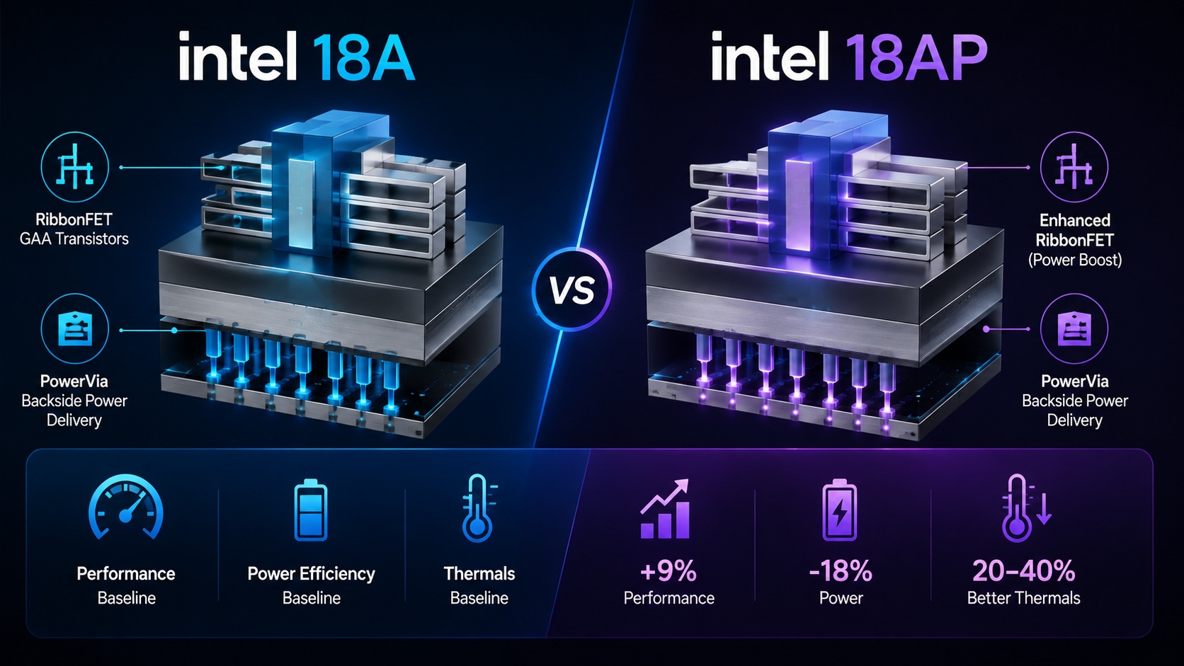 Intel 18A vs Intel 18A-P: What Is the Difference and Why Does It Matter?Intel’s 18A process technology has become one of…Read More
 WEBINAR: Why Google Cloud NetApp Volumes Matter for Modern EDA WorkloadsIn this webinar, Google Cloud and NetApp explore…Read More
 How to Free Yourself from Inconsistent Engineering Documentation Before It’s Too LateEmbedded systems programs often fail because critical engineering…Read More
2014 Semiconductor Growth Could be 2X 2013 Rate
The fourth quarter 2013 semiconductor market declined 0.8% from the third quarter, according to World Semiconductor Trade Statistics (WSTS). Full year 2013 growth was 4.8%. Our most recent 2013 forecast at Semiconductor Intelligence was 6% in November 2013, based on expectations of positive growth in 4Q 2013. Who had the most… Read More
6 reasons Synopsys covets C/C++ static analysis
By now, you’ve probably seen the news on Synopsys acquiring Coverity, and a few thoughts from our own Paul McLellan and Daniel Payne in commentary, who I respect deeply – and I’m guessing there are many like them out there in the EDA community scratching their heads a little or a lot at this. I’m not from corporate, but I am here… Read More
Mounir Hahad Rejoins Silvaco

Mounir Hahad just joined Silvaco as VP engineering. And when I say joined I really mean rejoined. I had a call with him to find out how that happened.
Mounir studied in France for a PhD in computer science on numerical computing. In 1995 the then-director of TCAD at Silvaco called him up having read some of his published papers. Silvaco… Read More
Before SPICE Circuit Simulation Comes TCAD Tools
I’ve run SPICE circuit simulators since the 1970’s and they use transistor models where the device parameters are provided by the foundry. These transistor and interconnect parameters come from an engineer at the foundry who has characterized silicon with actual measurements or by running a TCAD (Technology CAD)… Read More
ISSCC: Analog-Digital Converter in FD-SOI
The International Solid-State Circuits Conference (ISSCC) was last week in San Francisco. Stéphane Le Tual, Pratap Narayan Singh, Christophe Curis, Pierre Dautriche, all from STMicroelectronics presented a paper on A 20GHz-BW 6b 10GS/s 32mW Time-Interleaved SAR ADC with Master T&H in 28nm UTBB FDSOI Technology… Read More
$1 Billion IP & VIP sales by 2017?
We are not talking about ARM Ltd., as the IP vendor has already passed the $1B sales in 2013. In fact, we are not talking about a single IP vendor; this $1B mark will be passed by two IP market segments: Interface and Verification IP. In fact these two segments are very close together. When an IP is developed to support a specific Interface… Read More
Synopsys Acquires Coverity
Synopsys announced this afternoon that they are acquiring Coverity for $375M subject to all the usual reviews.
There are a couple of other big EDA connections. Aki Fujimora, who was CTO of Cadence, is on the board. And Adreas Kuehlmann is the VP of R&D. He used to run Cadence Berkeley Laboratories before moving to the other end… Read More
One SPIE session not to miss
The time is nigh for another meeting of the practitioners of the lithographic arts, dark and otherwise, at the SPIE Advanced Lithography symposium.
I love this conference for the engagement you see, both in the sessions and in the hallways. People actually meet and talk and argue. There’s always interesting gossip, exciting technologies,… Read More
Xilinx: Delivering a Generation Ahead
Last week was Xilinx’s investor day. Xilinx believe they are now a process generation ahead. They did over $100M in 28nm designs in FY2013 (Xilinx FY ended March 2013) and did over over $100M in Q4 2013 calendar year alone (and this is almost all true production volume, with only about 5% prototypes) with a plan greater than … Read More
Why Huawei Says It Will Match TSMC’s Most Advanced Chips by 2031