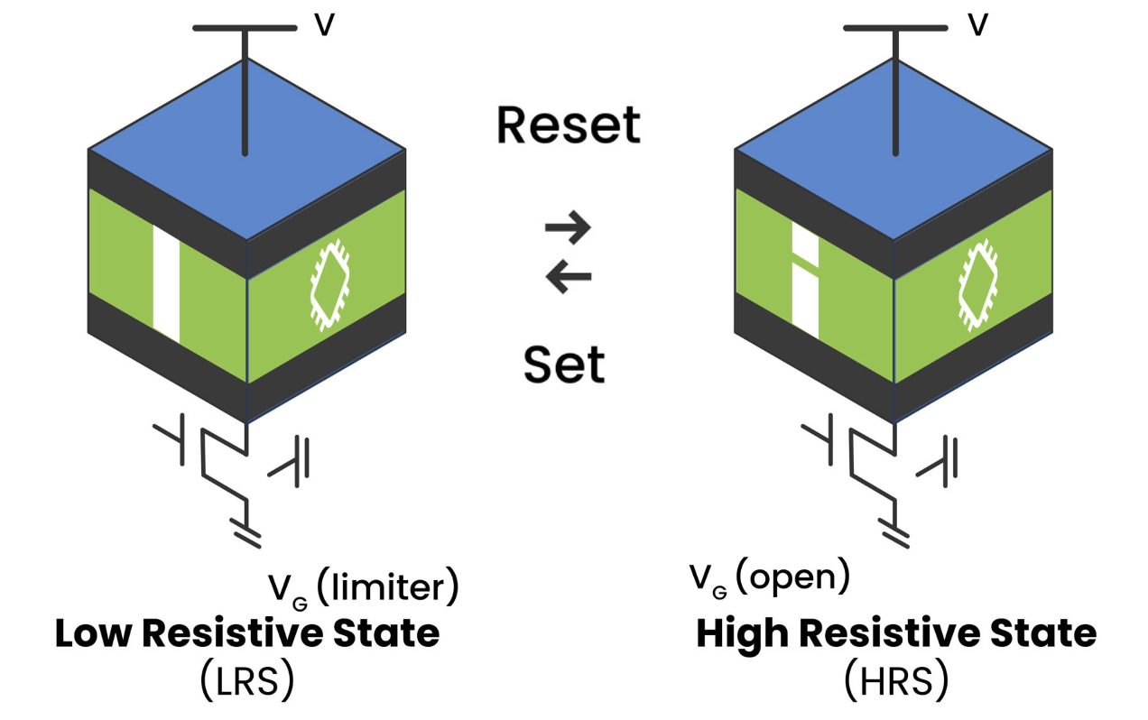
It’s well known that flash is the embedded non-volatile memory (NVM) incumbent technology. As with many technologies, flash is bumping into limits such as power consumption, speed, endurance and cost. It is also not scalable below 28nm. This presents problems for applications such as AI inference engines that require embedded NVM, typically on a single SoC below 28nm. Resistive random-access memory, referred to as ReRAM or RRAM, is emerging as the preferred alternative to address these shortcomings. Weebit Nano is paving the way for this change. Dan Nenni provides a good overview of the company’s ReRAM technology in this DAC report. The movement is gaining speed. In this post, I’ll review how things are coming together and how Weebit Nano is at the epicenter of the ReRAM revolution.
The Times Are Changing
At the recent TSMC Technology Symposium, there was a lot of discussion about ReRAM. Indeed, the foundry market leader (who refers to it as RRAM) talked up the technology in its presentation on embedded NVM. The company shared that RRAM, non-volatile memory well formed between backend metal layers, is an excellent Flash replacement with good scalability.
According to the TSMC website, TSMC continues to explore novel RRAM material stacks and their density-driven integration, along with variability-aware circuit design and programing constructs to realize high-density embedded RRAM-based solution options for AIoT applications.
Tech Insights recently reported that Nordic Semi’s new Bluetooth 5.4 SoC has 12 Mb embedded ReRAM on board. The piece went on to say that with multiple resistive states, which can correspond to multiple memory states, ReRAM is a leading contender for machine learning designs. Nordic’s chip is fabricated in TSMC 22 nm ultra-low leakage (22ULL) with an embedded resistive random-access memory (eReRAM) process.
According to the Yole Group by 2028, the total embedded emerging non-volatile memory market is expected to be worth ~$2.7 billion. Yole cited the first microcontroller product for automotive applications employing embedded RRAM from Infineon as an example of RRAM momentum. The Infineon AURIX TC4 MCU includes 20 MB of non-volatile resistive memory and is manufactured by TSMC in a 28nm process.
Another market research firm, Objective Analysis in its EMERGING MEMORIES BRANCH OUT report, states that over time, the NOR embedded in most SoCs will be almost entirely replaced by either MRAM, ReRAM, FRAM, or PCM.
This momentum isn’t limited to TSMC. On July 31 of this year, it was announced that Weebit Nano and DB HiTek tape-out ReRAM module in DB HiTek’s 130nm BCD process. It was reported that the demo chips will be used for testing and qualification ahead of customer production and demonstrate the performance and robustness of Weebit Nano’s ReRAM technology. And there’s more. Read on…
More From a Recent Memory Conference

Embedded non-volatile memory technology isn’t the only thing experiencing change. Conference names are evolving as well. The Design Automation Conference is now DAC: The Chips to Systems Conference. The Flash Memory Summit is now FMS: the Future of Memory and Storage. At that conference, which was held in Santa Clara from August 6-8, 2024, Weebit Nano’s VP of Quality and Reliability Amir Regev gave a presentation on emerging memories. During that presentation, Amir presented more evidence of the ReRAM revolution.
Amir presented test results for Weebit’s ReRAM technology implemented on GlobalFoundries 22FDX wafers. This is significant as this is the first time any public data has been shared about NVM performance at nodes such as 22nm.You can read the press release announcing this milestone here. In that release, it was reported that, Mr. Regev will also highlight the performance of Weebit ReRAM on GlobalFoundries 22FDX® wafers including endurance and retention data – the first such ReRAM results.
Here are some details that Amir presented:
- Earlier this year Weebit received GF 22FDX wafers incorporating our ReRAM module prototype
- 8Mb, 128-bit wide, targeting 10K cycles and 10yr retention at 105°C (automotive to follow)
- Characterization and qualification activities are ongoing
- Pre-qualification results show:
- Weebit’s ReRAM stack is stable at 105°C cycling endurance up to 10K cycling
- Very good data retention pre- and post-cycling is maintained for a long time at high temperatures (150°C), as shown in the figure below.

Amir also provided a broad summary of Weebit’s qualification work:
- Qualified modules at 85°C and 125°C
- Temperatures specified for industrial and automotive grade 1 ICs
- Qualified for endurance and 10yr retention per JEDEC industry standards
- AEC-Q100 qualification (150°C and 100K cycles) in progress
- Good results achieved, collecting statistical data for full qualification
- Technology demonstrated on multiple process nodes
- From 130nm to 22nm, Al / Cu, 200mm / 300mm
- Successfully simulated on FinFET nodes
Amir also described the work underway to qualify Weebit’s ReRAM under extended automotive conditions. He mentioned the excellent results so far on temperature cycling provide a strong foundation for automotive qualification.
Weebit Nano’s ReRAM is finding application in a wide range of processes, foundries and applications. Beyond those mentioned so far, the company also recently announced work with Efabless on SkyWater’s 130nm CMOS (S130) process. This work enables fast and easy prototyping of intelligent devices using Weebit’s technology. Weebit Nano is creating a wide footprint in the market.
To Learn More
ReRAM technology is poised to change the game for many applications. If your next project includes embedded non-volatile memory, you should see how Weebit Nano can help. You can learn more about the company’s technology here. If you want to chat with the Weebit team, you can start here. Weebit Nano is at the epicenter of the ReRAM revolution, join in.
Share this post via:


Comments
3 Replies to “Weebit Nano is at the Epicenter of the ReRAM Revolution”
You must register or log in to view/post comments.