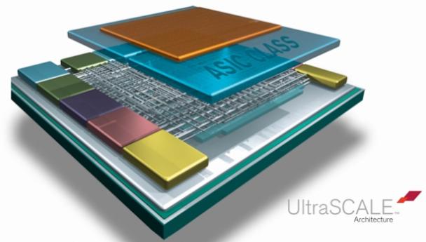
This week Xilinx has announced that “The Xilinx 20nm All Programmable UltraScale™ portfolio is now available with detailed device tables, product documentation, design tools and methodology support.”

Do you know what 20nm is? It’s small, tiny. Think about it this way, as I just learned today that one nanometer is about as long as your fingernail grows in one second, so in 20 seconds… there you go another channel length goes by. I know what you all just did… You just looked at your finger nails did not you?? Maybe some of you chewed on them, I looked.
Also read: Xilinx Begins Shipping TSMC 20nm FPGAs!
Before I continue, let me explain some language that has changed slightly as not to confuse my dear readers. We are used to the Virtex-5,6,7 nomenclature but the ‘8’ is not to be. It has morphed into UltraScale, as this 20nm node is simply not a device shrink. UltraScale 3D FPGAs contain a step-function increase in both the amount of connectivity resources and the associated inter-die bandwidth in this second-generation 3D IC architecture. The big increase in routing and bandwidth and new 3D IC wide memory optimized interface ensures that next-generation applications can achieve their target performance at extreme levels of utilization. The other change is that the DSP rich devices are in the Kintex family and the Virtex family will be GT rich. Bottom line here, is there is an UltraScale FPGA that is going to meet your massive, insatiable, intense design, or maybe you’re not so large design. Either way Xilinx has you covered as always. Below is what the Kintex UltraScale has to offer. Click here to get the whole story.

The Power of the Xilinx FPGA is the reprogrammability of the FPGA. Yes, all FPGAs are reprogrammable but Xilinx has innovated in how one programs BILLIONS of transistors to produce a particular function or design. That is not a trivial task. A decade ago, when FPGAs were considerable smaller, using VHDL or Verilog was reasonable then followed by RTL simulations. This model is no longer effective if one is to beat their competitors in time to market. Think about it, can we really hand code an FPGA in a reasonable amount of time that has billions of transistors? I believe no, not reasonable in QOR, Cost and Schedule. Not that there are not great FPGA designers (is that a double negative?) but the problem lies with what is happening in the industry. Systems that used to contain racks and racks of FPGA boards are reduced down to a set of FPGA boards. The Interface layer collapses, memory, power, system integration time and cost etc… So how did Xilinx get here, being the leader in the FPGA, ASIC Class devices?
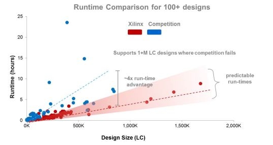
If Xilinx just created a 20nm device and made no changes to the tools that program and route the device, we would have a very flashy paper weight. Xilinx in parallel with the silicon design has retooled and created the ‘Vivado’ design tool suite. ISE is no longer for the UltraScale FPGAs. Vivado is the center of the UltraScale FPGA programmability. What this means for the FPGA designers is the confidence that you can really utilize the UltraScale FPGA to 90%+ and still meet timing closure that no longer takes a day but hours.

For us FPGA designers, that is a big deal. As if that is not enough Xilinx has opened up on how one can program the FPGA. C/C++, SystemC, OpenCL, MATLAB etc… And of course still VHDL/Verilog when necessary, for example top level design wrappers. Vivado HLS, as I have written before will allow the user to explore and design the UltraScale FPGA faster than ever. I encourage you to check out all the papers, videos, IP, Cores, Libraries, and resources about Xilinx’s ground breaking 20nm UltraScale FPGAs, you will not be disappointed, but wishing for an evaluation board today at Xilinx.com
lang: en_US
Share this post via:


Musk’s Orbital Compute Vision: TERAFAB and the End of the Terrestrial Data Center