Array
(
    [content] => 
    [params] => Array
        (
            [0] => /forum/threads/intel-provides-update-on-internal-foundry-model.18234/
        )

    [addOns] => Array
        (
            [DL6/MLTP] => 13
            [Hampel/TimeZoneDebug] => 1000070
            [SV/ChangePostDate] => 2010200
            [SemiWiki/Newsletter] => 1000010
            [SemiWiki/WPMenu] => 1000010
            [SemiWiki/XPressExtend] => 1000010
            [ThemeHouse/XLink] => 1000970
            [ThemeHouse/XPress] => 1010570
            [XF] => 2021770
            [XFI] => 1050270
        )

    [wordpress] => /var/www/html
)

Intel Provides Update on Internal Foundry Model

Daniel Nenni

Admin
Staff member
Intel Internal Foundry Model.jpg


New model represents fundamental change to operations aimed at unlocking significant value.

Intel leaders told analysts and investors during a webinar Wednesday that its transition to a new internal foundry model will be a key enabler to achieving its stated cost savings goal of more than $8-10 billion exiting 2025. In this new operating model, Intel’s internal product groups move to a foundry-style relationship with the company’s manufacturing group. As a result, company execs say they are projecting a broad class of increased efficiencies that will be reflected in greater profitability as Intel pursues its long-term ambition to achieve non-GAAP gross margins of 60%.

The Background:
Intel is embarking on the most significant business transformation in its 55-year history. With IDM 2.0, Intel set out to regain process technology leadership, expand the use of third-party foundry capacity and build a world-class foundry business with a significant expansion of Intel’s manufacturing capacity. With these efforts well on track, Intel now is making a fundamental shift in how its product business units work with technology development and manufacturing to ensure long-term growth while achieving efficiencies and cost savings.

In this new “internal foundry” model, Intel’s product business units will engage with the company’s manufacturing group in a similar arm’s-length fashion that fabless semiconductor companies engage with external foundries.

Intel’s internal foundry model is key to the company’s overarching IDM 2.0 strategy — with the aim to return margins to their historic range and ambitions to serve a far wider variety of chip customers worldwide. The internal foundry model is also integral to Intel’s multiyear cost efficiency effort, which includes reducing costs by $3 billion in 2023, and $8 to $10 billion in cost savings exiting 2025 – which is where the new model plays a significant role.

David Zinsner, Intel Executive Vice President and Chief Financial Officer, and Jason Grebe, Corporate Vice President and General Manager of Intel’s Corporate Planning Group, hosted a webinar on Wednesday for investors and analysts. The event’s purpose was to explain the internal foundry model and its many benefits, and share its implications for Intel’s culture, competitiveness, financials – and, ultimately, its transformation.

Here are the key takeaways from the webinar. The event replay is available here, along with the accompanying slides.

Driving Value with Intel’s Internal Foundry Model

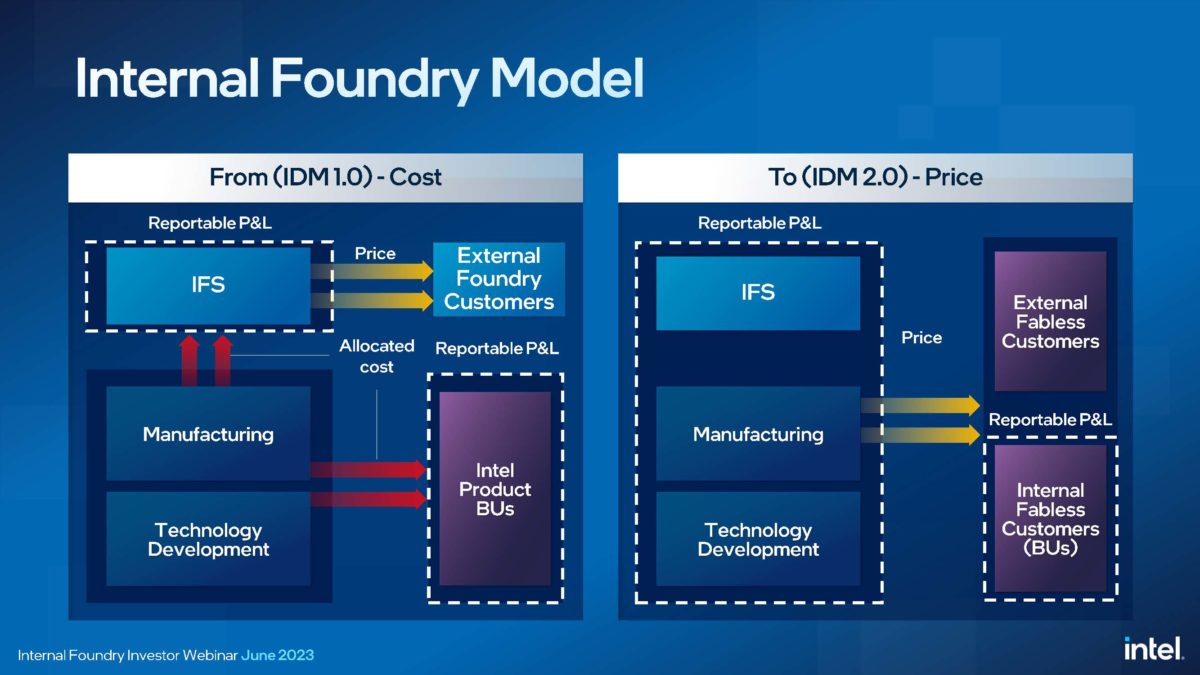
In its new operating model, Intel’s manufacturing groups will be accountable to a standalone profit and loss (P&L) for the first time. Beginning in Q1 2024, the reportable P&Ls will include a new manufacturing group segment – inclusive of manufacturing, technology development and Intel Foundry Services (IFS) – along with the company’s product groups – Client Computing, Data Center and AI, Network and Edge, and All Other.

The internal foundry model offers significant inherent business value beyond billions of dollars in cost savings. Intel will extend the use of market-based pricing to its internal business units, offering them the same certainty and stability as the company’s external customers. Intel will maintain the intimacy and deep connection between its product groups and technology development teams, preserving the competitive advantages it has had as an IDM. The new model also provides a tailwind to IFS by effectively creating the industry’s second-largest foundry (by volume from internal customers), allowing external customers to build off Intel’s internal scale and de-risking the process.

Intel’s manufacturing groups will face the same market dynamics as their external foundry counterparts and need to compete for volume through performance and price. This includes Intel’s internal customers, who will have the flexibility over time to engage with third-party foundries. It’s not an entirely new notion for Intel, however; today, roughly 20% of Intel’s silicon is manufactured externally.

“The semiconductor industry and computing in general have evolved rapidly, and we need to adjust our business operations in response. With the advent of smartphones, the digital network, the intelligent edge, cloud computing and AI, compute demands have diversified,” said Zinsner.

Supporting Long-Term Margin Ambitions

Intel’s long-term ambitions are to achieve non-GAAP gross margins of 60% and operating margins of 40%. The internal foundry model will highlight new opportunities and lead to an optimized cost structure in furtherance of these goals.

Intel has highlighted before its ambitions to be the second largest external foundry by 2030, which continues to be its goal. In its new model, based off internal volume, the company expects to be the second largest foundry next year – with manufacturing revenue greater than $20 billion.

“We’ve already done a lot of internal analysis and benchmarking to identify areas of opportunity,” said Grebe.

The internal foundry model will offer strong incentives for Intel business groups to work even more efficiently. For example, “expedited” wafers that business units decide to move through Intel’s manufacturing process are costly and reduce factory efficiency. Going forward, this service charge will be borne by the business units, and it’s expected that it will reduce the number of expedites to be on par with the competition.

Already Uncovered: Specific Examples of Internal Foundry Model Benefits

“We have identified many opportunities for optimization across both our manufacturing organizations and our business units that will lead to significant saving,” Grebe continued.

For example, cost and efficiency savings from fewer expedited wafers moving through the factories are expected to deliver annual savings over time in the range of $500 million to $1 billion.

Also, Intel’s test times currently run double or triple those of competitors. As business units are charged market prices based on test time, Intel expects pre-silicon design choices to reduce these test times, eventually producing savings of approximately $500 million annually.

And by reducing the number of wafer steppings, the number of physical iterations of a product’s design, the company estimates it will realize cost savings in the $500 million to $1 billion range.

Creating a ‘Tailwind’ for IFS

By creating, with internal customer volume, what will effectively be the world’s second-largest foundry, Intel will provide a scale and manufacturing tailwind for its IFS business.

First, by establishing the manufacturing organization as its own business and ensuring it has the decision rights to manage its P&L, Intel will be able to allocate clear corridors of capacity and supply commitments to external customers.

Also, because the internal foundry model is an arm’s-length approach that increases the independence of the manufacturing organizations, Intel will deliver complete segregation for foundry customers’ data and IP.

“As we begin retooling the company for this transformation, we are architecting with a security-first mindset, taking data separation as a key tenet into our system design,” Grebe noted.

Importantly, customers also expect world-class foundry service levels. As part of its shift to the internal foundry model, Intel is building the service-oriented mindset that is required to be a key player in the foundry business. Both Intel’s manufacturing group and IFS are benchmarking themselves against industry peers to ensure Intel is on track to provide best-in-class service levels expected from a foundry.

Lastly, more than five internal products are presently being developed on Intel’s latest 18A process technology, which is expected to come to market in 2025. This process node will initially ramp on internal volume, allowing any process issues to be addressed, and as a result will largely de-risk the new process for external IFS customers.

Establishing an internal foundry model is one of the most significant steps Intel is taking to deliver IDM 2.0 as it fundamentally changes the way the company operates and establishes the structure and incentives needed to drive a change in culture and new behaviors. As it leverages industry standard planning processes, data management strategies, systems and tools, Intel is building the foundation to be both a world-class IDM and foundry provider. Additionally, giving the manufacturing group its own P&L, along with the associated transparency and accountability, will be a key driver in achieving Intel’s target of reducing $8 to $10 billion in costs and achieve its long-term profit goals. Finally, the internal foundry model will be a strong tailwind to the company’s IFS strategy.

 
Last edited:
During the call, Intel declared it is (or soon will be) the second largest foundry in the world with $20 billion revenue. The majority of the $20 billion revenue is coming from Intel internal fabless design divisions.
 
During the call, Intel declared it is (or soon will be) the second largest foundry in the world with $20 billion revenue. The majority of the $20 billion revenue is coming from Intel internal fabless design divisions.

Yes, Intel will be counting internal products just like Samsung. It is an apple to apple IDM foundry comparison which is fair game. The Samsung Foundry Day is next week so perfect timing.

Samsung Foundry Forum
 
Here is a slide worth talking about:

View attachment 1259

At this important IFS conference call, Intel assigned Intel CFO with accounting/finance background and one vice president in corporate planning with sales/marketing background to explain this and several other technical oriented slides. Are those executives at IFS too busy to be invited to promote themselves?
 
 
For whatever reasons INTC fell 6% in aftermarket trading following this update on IFS. I didn't see anything very negative, other than the gross margin numbers which were already known. Weird.
 
What is it about expedited wafers that cost $500M to 1B? I thought the manufacturing machinery iremains fully utilized, you just jump the queue. So you pay compensation to someone for delay (or the foundry charges you more for the privilege, same thing). So are they talking about having that much waste in how they use external fabs today?

And reducing wafer steppings - huh? What causes that to happen just because they have more fabs?
 
so that Intel 3 vs TSMC 3nm and Intel 20A vs TSMC 3nm is kind of interesting. Instead of comparing 20A to N2, it compare 20A with N3
That's because 20A probably performs worse than N3.
Moore's law leaked the Arrow lake product line out and it had the i9/i7 performance products on N3 and budget i5/i3 on 20A.
 
That's because 20A probably performs worse than N3.
Moore's law leaked the Arrow lake product line out and it had the i9/i7 performance products on N3 and budget i5/i3 on 20A.
well, it should perform better than N3 considering 20A has both PowerVia and RibbonFET available, and 18A is just a refinery compared to 20A. So 20A is better than N3 for sure in terms of high performance.

I wouldn't take MLID's word for granted since leaks can be misinformative sometimes and can sometimes hide the real reason. I would rather believe that Intel may rely on N3 because of capacity issues and yield. I don't think that planned capacity for 20A/18A will go online and be available in late 2024. So, I believe they have limited capacity for arrow lake until Arizona's Fabs are fully operational.

They have a very intense schedule considering that those fabs will be online 2024, and we don't know if it's coming in first half or second half. But those 2 fabs in Arizona will likely be in latest 18A class considering the budget increased from 20B to 30B.
 
well, it should perform better than N3 considering 20A has both PowerVia and RibbonFET available, and 18A is just a refinery compared to 20A. So 20A is better than N3 for sure in terms of high performance.
Well, it should perform better, but the devil is in the details. It could be that as they are trying to rush the GAA to market ahead of everyone else they are willing to accept a poorer parametric yield.
Also, Moore's law leaks have proved to be accurate in the past. He correctly predicted that Sierra Forest would release before granite rapids and have 144 cores.
I don't think that planned capacity for 20A/18A will go online and be available in late 2024.
I don't think so either... but if 20A isn't ready in 2024, 18A is unlikely in 2025
 
For whatever reasons INTC fell 6% in aftermarket trading following this update on IFS. I didn't see anything very negative, other than the gross margin numbers which were already known. Weird.

There was nothing new except they mentioned that the 18A PDKs were not ready yet thus no customer announcement. We have talked about that on SemiWiki but maybe it was not known to outsiders. They said the 18A PDKs should be done in the second half of 2023. Hopefully that is true. If not TSMC will sweep the top semiconductor companies once again.

The other thing, as was posted here, nobody from IFS was on the call which was a mistake. Stuart Penn should have been on it. I realize it was an investor call but someone from IFS should have been there, my opinion. Even if it was a prepared/pre-recorded piece like the others.

Otherwise it was professionally done and the Q&A went well. There seems to be a lot of pressure to announce 18A customers and that could be a big hit if there are none by the end of the year. You can bet the IFS people are out there hugging TSMC's top customers. My bet is Nvidia, MediaTek, Microsoft, Google, Amazon, Broadcom, QCOM, and Marvell.

I'm confident they will get customers but those companies will also use TSMC N2 to mitigate risk so there will be no home runs per say.
 
Well, it should perform better, but the devil is in the details. It could be that as they are trying to rush the GAA to market ahead of everyone else they are willing to accept a poorer parametric yield.
Also, Moore's law leaks have proved to be accurate in the past. He correctly predicted that Sierra Forest would release before granite rapids and have 144 cores.

I don't think so either... but if 20A isn't ready in 2024, 18A is unlikely in 2025
yeah, we won't know for sure until arrow lake come to market. Same with meteor lake that still confuse many people
 
That's because 20A probably performs worse than N3.
Moore's law leaked the Arrow lake product line out and it had the i9/i7 performance products on N3 and budget i5/i3 on 20A.

The comparison was timing (release date), not performance or density. The problem with that is how do you define release date? For TSMC it is an Apple SoC which means a very large and complex chip manufactured by the millions. Intel 20A is Intel designed CPU chiplets. A very different event, absolutely. And yes if Intel can't yield chiplets at 20A they will probably have a problems with full chips at 18A. Exciting times for sure. GO IFS!
 
During the call, Intel declared it is (or soon will be) the second largest foundry in the world with $20 billion revenue. The majority of the $20 billion revenue is coming from Intel internal fabless design divisions.
As long as they continue to break out the external foundry number like Dave said on the call, I don't see any problem with this. The way I see it it is more information on how intel is doing and how TD-MSO-IFS (TMI) is meeting internal demands, and how IFS is doing.
That's because 20A probably performs worse than N3.
Moore's law leaked the Arrow lake product line out and it had the i9/i7 performance products on N3 and budget i5/i3 on 20A.
Based on VSLI last year, it seems likely intel 4 is performance competitive with N3 and very likely N3E. Intel 4+power via is +6% fmax and lower power. Unless 20A's FEOL is a more than 6% regression on intel 4, I don't know how that is physically possible.
Otherwise it was professionally done and the Q&A went well. There seems to be a lot of pressure to announce 18A customers and that could be a big hit if there are none by the end of the year. You can bet the IFS people are out there hugging TSMC's top customers. My bet is Nvidia, MediaTek, Microsoft, Google, Amazon, Broadcom, QCOM, and Marvell.

I'm confident they will get customers but those companies will also use TSMC N2 to mitigate risk so there will be no home runs per say.
Do you think pulling away the cover over the intel 3 customer (in a similar manner to what happened with the MTK announcement for smartTV chips) would be something that would boost investor confidence? My guess is no given the smaller $4B of the deal, and that all the investment community seems to care about is 18A (I think somewhat rightfully so). I think on the Q1 earnings call they said they would reveal more about that deal during the 2H of the year, hopefully it is at the foundry meeting that is also supposed to be happening 2H23 alongside the 18A customer they hope to nab. And while I'm at it, I want a detailed intel 3 and 20A paper at IEDM underneath my Christmas tree :).
 
Back
Top