Array
(
    [content] => 
    [params] => Array
        (
            [0] => /forum/threads/gloablfoundries-making-chips-for-the-s6-i-think-so.5836/
        )

    [addOns] => Array
        (
            [DL6/MLTP] => 13
            [Hampel/TimeZoneDebug] => 1000070
            [SV/ChangePostDate] => 2010200
            [SemiWiki/Newsletter] => 1000010
            [SemiWiki/WPMenu] => 1000010
            [SemiWiki/XPressExtend] => 1000010
            [ThemeHouse/XLink] => 1000970
            [ThemeHouse/XPress] => 1010570
            [XF] => 2021770
            [XFI] => 1050270
        )

    [wordpress] => /var/www/html
)

Gloablfoundries making chips for the S6? I think so...

mustache143

New member
While confirmation came over the Easter weekend that Globalfoundries 14nm finfet process was in full production ramp, it was the Chipworks tear down of a retail S6 that caught my attention.

Inside the Samsung Galaxy S6 | Chipworks Blog

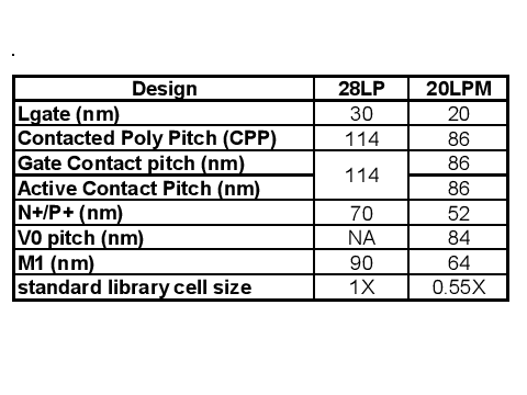
It seems Global may actually be making some of the chips for the S6, as indicated by the marking on the retail chip itself. Living in Albany, I can say the barroom buzz would confirm this. Perhaps Samsung needed additional fab capacity or this chip at ~78sq-mm is a good process validation chip for the copy-'almost exact' that Samsung and GF are using. I'd be interested in people's opinion on the shrink from the 20-nm 5433 to the 14-nm finfet 7420 from ~113 to ~78mm. Definitely not just 20nm with finfet... although denser libraries could have helped a lot.
 
I have not seen BEOL numbers on the Samsung 20nm process but Samsung 14nm is pretty much identical on the back end as TSMC 20nm. The poly to gate pitch is a bit tighter but the rest is the same. Maybe Scott Jones can weigh in here, I'm sure he knows.

That does not mean that the foundation IP (SRAM, STD Cells, IOs) will be created equal. We should see a silicon comparison between 14nm and 16FF+ in the second half, until then we can only speculate.

The trend amongst the media has certainly changed to Samsung having the A9 but as I mentioned before that decision was made a long time ago. It is Samsung 14nmLP for the A9 and TSMC 16EFT for the A9x.

GF has a copy exact Samsung 14nm process which, contrary to FUD, is ramping as planned so Apple and QCOM can get wafers there as well.

I'm still trying to find out what GF will do for 10nm. Copy exact Samsung or use the IBM 10nm version. My guess is the latter which is not being disclosed due to the acquisition quiet period. Have you heard anything in Albany?
 
Last edited:
Daniel,

I haven't heard a peep on 10nm. As best I can tell, it has been all hands on deck scramble to be first with 14nm. I knew there was a lot of FUD in the media, I guess it was just a welcome relief this morning to see a retail phone with a 14nm Globalfoundries chip inside. Given the millions of S6s being produced, I'd take it to the bank that the hoopla of GF being way behind was just a bunch of hot air. Retail product teardowns don't lie.

As for 10nm... not a peep...
 
I have not seen BEOL numbers on the Samsung 20nm process but Samsung 14nm is pretty much identical on the back end as TSMC 20nm. The poly to gate pitch is a bit tighter but the rest is the same. Maybe Scott Jones can weigh in here, I'm sure he knows.

That does not mean that the foundation IP (SRAM, STD Cells, IOs) will be created equal. We should see a silicon comparison between 14nm and 16FF+ in the second half, until then we can only speculate.
The IP improvement must be massive for the chip to shrink that much.

From the 5433 to the 7420 they have (confirmed so far):

- Went from LPDDR3 to LPDDR4 controllers
- Removed a dedicated HEVC decoder
- Added HEVC decoding and encoding capability to their MFC media block
- Increased the GPU clusters from 6 to 8.

Plus many other changes we still have to wait on to confirm.

Yet they managed to shrink the die size from 113mm² to 78mm²?

For reference, here is a floor plan of the 5433 as published by Samsung: http://pc.watch.impress.co.jp/img/pcw/docs/694/058/01.png

Also, these are supposedly the 20LPE and 20LPM numbers from ISSCC: ??????Weekly???????Samsung?Galaxy????????????SoC?Exynos? - PC Watch

06.png

05.png
 
Last edited:
Actually re-reading the translation of the ISSCC presentation things seem to be more clear:

The 5433 is a 20LPE product with 80nm M1x. Samsung's 14LPE process takes the BOEL from the 20LPM process though which has a 64nm M1x, which explains the large shrink.

Given the rough GP*M1x formula:

20LPE: 7200
20LPM: 5504
14LPE: 4992 (Assuming 78nm GP)

20LPE/14LPE = 1.44x shrink.

113mm² / 1.44 = 78mm². I know that's a stupid coincidence that doesn't explain the added complexity of the SoC such as 2 more GPU clusters, but at least we're getting nearer to reality.
 
Actually, there is no definate confirmation that it's manufactured at Globalfoundries. All we have is some speculation based on the letters on the package:
Could ALB be short for Albany (NY)? Is the G in the lot code short for GLOBALFOUNDRIES?
That's hardly conclusive.
 
Actually, there is no definate confirmation that it's manufactured at Globalfoundries. All we have is some speculation based on the letters on the package:

That's hardly conclusive.

I just thought about it. Albany is the capital of New York state and is more famous to many people. But Globalfoundries fab is actually located in Malta, NY. Malta is in Saratoga County NY and Albany is in Albany county NY. It takes a 30-minute/28 miles drive to travel between these two places. Globalfountries' website stated their Fab 8 is in Malta NY or Saratoga County NY. Can they say any products they made in Fab 8 are "Made in Albany"? It's bit strange to me.
 
I just thought about it. Albany is the capital of New York state and is more famous to many people. But Globalfoundries fab is actually located in Malta, NY. Malta is in Saratoga County NY and Albany is in Albany county NY. It takes a 30-minute/28 miles drive to travel between these two places. Globalfountries' website stated their Fab 8 is in Malta NY or Saratoga County NY. Can they say any products they made in Fab 8 are "Made in Albany"? It's bit strange to me.

While, it is speculation that this particular chip was manufactured at GF's NY fab it is not unreasonable to associate ALB with Malta and any other factory in the 'capital region'. Locals here really don't delineate between Albany, Schenectady, Troy and Saratoga as they are all considered the 'capital region'. As for the ALB abbreviation, whenever you get a package delivered to your home via air transport it is marked with ALB as it is the FAA designation for the regional airport. ALB is the air cargo hub for Malta and any USPS, FedEx, UPS etc package has ALB stamped on it in very large letters. I would find it quite a coincidence that three random letters were chosen for a chip marking which also are the exact letters for the air cargo hub of a fab which is known to be producing 14nm finfet chips. In fact, the odds are mighty small that ALB was randomly chosen as an identifier out of the thousands of other possible combinations. If I were I betting man, I would put a lot of money on the fact that this chip was indeed made in Malta. That is besides the fact that I got a nice little silent confirmation smirk when I asked a friend point blank if it came out of his fab.
 
While, it is speculation that this particular chip was manufactured at GF's NY fab it is not unreasonable to associate ALB with Malta and any other factory in the 'capital region'. Locals here really don't delineate between Albany, Schenectady, Troy and Saratoga as they are all considered the 'capital region'. As for the ALB abbreviation, whenever you get a package delivered to your home via air transport it is marked with ALB as it is the FAA designation for the regional airport. ALB is the air cargo hub for Malta and any USPS, FedEx, UPS etc package has ALB stamped on it in very large letters. I would find it quite a coincidence that three random letters were chosen for a chip marking which also are the exact letters for the air cargo hub of a fab which is known to be producing 14nm finfet chips. In fact, the odds are mighty small that ALB was randomly chosen as an identifier out of the thousands of other possible combinations. If I were I betting man, I would put a lot of money on the fact that this chip was indeed made in Malta. That is besides the fact that I got a nice little silent confirmation smirk when I asked a friend point blank if it came out of his fab.

We don't need to bet our money on this :). Just wait for some more days or weeks we will know the truth.

No matter where the new Samsung chips are made, my wife and I enjoyed our time spent in Albany almost 30 years ago. Albany was a little bit strange to us at beginning. It's a small town (<100,00 population) but it's also a college town, the capital of New York, a hub of many culture and history events and sites. The downtown State building, musical hall, museums, and many other things are unusual for a small town of this size. The city's economy is heavily linked to public sector's activity. Several years ago we heard Key Bank moved their headquarters from Albany to Cleveland, Ohio because there're not enough commercial flights serving Albany. My wife felt it's sad because she got her first ATM card from Key Bank in Albany.

This January we had a chance to visit friends around Albany and we drove to Malta to take some pictures.

View attachment 13840View attachment 13841View attachment 13842View attachment 13843View attachment 13844View attachment 13845View attachment 13846View attachment 13847
 
Last edited:
GF if they are making these(I'm very doubtful.The A is more likely Austin) is making them in very small #'s.
 
There's a new statement from Globalfoundries:
Our 14nm FinFET technology is maturing and on schedule at our Fab 8 facility in Malta, New York,” said Jason Gorss, a spokesman for GlobalFoundries, in a statement. “The early version (14LPE) is qualified in our fab and our lead product is yielding in double digits. Since 2014, we have taped multiple products and testchips and are seeing rapid progress, in yield and maturity, for volume shipments in 2015.”
GlobalFoundries: Our lead 14nm product is yielding in double digits | KitGuru
"Yielding in double digits" - usually when people say double digits they mean in the teens, i.e 10 -20%. Isn't that a pretty poor yield?
 
This statement looks like it was released in 2014.

As nebulous as this statement is, more telling is that Malta is still running extremely small volumes.
 
This statement looks like it was released in 2014.

As nebulous as this statement is, more telling is that Malta is still running extremely small volumes.
That's even more nebulous to me. What do you mean for extremely small volumes?
 
That's even more nebulous to me. What do you mean for extremely small volumes?
They might still be using the 7420 as a pipe-cleaner to get yields up.

For one I'm now convinced the ALB tag has nothing to do with Albany, previous packages contained the markings ACA, BEB, AJB, AKD, all similar enough to make ALB just a coincidence.

Also Samsung does their own Exynos packaging with DRAM in-house, so having GF fab a large quantity for the S6 seems logistically unintuitive.
 
I have not seen BEOL numbers on the Samsung 20nm process but Samsung 14nm is pretty much identical on the back end as TSMC 20nm. The poly to gate pitch is a bit tighter but the rest is the same. Maybe Scott Jones can weigh in here, I'm sure he knows.

That does not mean that the foundation IP (SRAM, STD Cells, IOs) will be created equal. We should see a silicon comparison between 14nm and 16FF+ in the second half, until then we can only speculate.

The trend amongst the media has certainly changed to Samsung having the A9 but as I mentioned before that decision was made a long time ago. It is Samsung 14nmLP for the A9 and TSMC 16EFT for the A9x.

GF has a copy exact Samsung 14nm process which, contrary to FUD, is ramping as planned so Apple and QCOM can get wafers there as well.

I'm still trying to find out what GF will do for 10nm. Copy exact Samsung or use the IBM 10nm version. My guess is the latter which is not being disclosed due to the acquisition quiet period. Have you heard anything in Albany?


GF does not have a "partner" on 10nm, so is proceeding on their own. Not copy exact from either place at this time. And they are a bit behind on the 14nm HVM, pushing hard to keep pace.
 
There is some speculation by nitwit-analyst Kuo that the 14nm yields at GF are pretty bad (30%):

Apple makes 'last-minute decision' to use TSMC for 30% of 'A9' chip orders for next iPhone

and 30% of the orders are back at TSMC.

Again makes no sense to me. IMHO any fab should be ashamed of themselves if they actually got 30% yield for a pretty much logic design (SRAM, ROM, standard-cell, bunch of PLLs, memory controllers, USB PHY etc). Furthermore, 50% yield to go into mass production ? Maybe I'm too long out of the semi-industry, but in "my days" >90% pre-assembly was a hard requirements or otherwise we didn't go into mass production at all.

Furthermore, I can't imagine Apple has two parallel teams for a SoC, one targetting GF/Samsung process, a 2nd team (backup) doing the same design for TSMC. Costs lots of money. Imagine the pain of the tapeouts, metal fixes, mask sets, different hard macro's etc.
 
Again makes no sense to me. IMHO any fab should be ashamed of themselves if they actually got 30% yield for a pretty much logic design (SRAM, ROM, standard-cell, bunch of PLLs, memory controllers, USB PHY etc). Furthermore, 50% yield to go into mass production ? Maybe I'm too long out of the semi-industry, but in "my days" >90% pre-assembly was a hard requirements or otherwise we didn't go into mass production at all.
90%??? At 14nm? I guess not even at the very end of the product lifetime.

Furthermore, I can't imagine Apple has two parallel teams for a SoC, one targetting GF/Samsung process, a 2nd team (backup) doing the same design for TSMC. Costs lots of money. Imagine the pain of the tapeouts, metal fixes, mask sets, different hard macro's etc.
I agree, but since we are talking about Apple, I wouldn't exclude that.
 
90%??? At 14nm? I guess not even at the very end of the product lifetime.

Guess I'm mistaken here, we needed >97% pre-test COVERAGE, not actual yield. About die yield, I vaguely recall >80% for a 180nm
process. Guess for much smaller nodes incl. all the matching issues with double patterning etc. that's a mission impossible these days
and the die yields are much lower.

Doing two parallel designs of a SoC is crazy, but then again maybe Apple is indeed playing games with the two foundries. Who at the end of Q1 has the best cost/yield/leakage etc. wins the production contract.
 
Back
Top