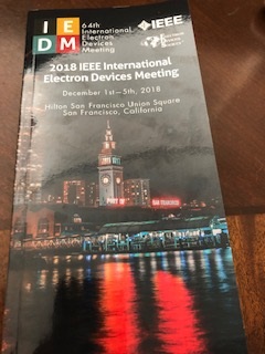
Hello, my name is Daniel Nenni and I am a semiconductor conference addict. I just can’t seem to get enough. The semiconductor ecosystem is very wide now and moves so quickly it is nearly impossible to keep up without constant conference attendance. As a SemiWiki contributor not only do I get free conference passes, I get access to people and materials that help feed my insatiable appetite for semiconductor information. The world really does revolve around semiconductors and now me personally since I know all that is semiconductor, absolutely.
Premier SemiWiki blogger Scott Jones also attended IEDM and will have more detailed blogs coming soon.
About IEDM
With a history stretching back more than 60 years, the IEEE International Electron Devices Meeting (IEDM) is the world’s pre-eminent forum for reporting technological breakthroughs in the areas of semiconductor and electronic device technology, design, manufacturing, physics, and modeling. IEDM is the flagship conference for nanometer-scale CMOS transistor technology, advanced memory, displays, sensors, MEMS devices, novel quantum and nano-scale devices and phenomenology, optoelectronics, devices for power and energy harvesting, high-speed devices, as well as process technology and device modeling and simulation. The conference scope not only encompasses devices in silicon, compound and organic semiconductors, but also in emerging material systems. IEDM is truly an international conference, with strong representation from speakers from around the globe.
As I mentioned before, IEDM is the premier semiconductor process technology conference. This year the theme is Device Breakthroughs from Quantum to 5G and Beyond. One of the more interesting topics to me was Interconnects to Enable Continued Scaling with papers from ARM, IBM, IMEC, UT Austin, GlobalFoundries, Stanford, and AMAT. This is a must read for those of you who think Moore’s Law (which is actually an observation) and semiconductor scaling is at an end, because it is not, not even close.
There was also an interesting session on 3D integration: High Density Stacked FinFETs and 3D integration of 2D memory. Memory technology was a major focus (especially MRAM), and rightly so, but I did not have time for it unfortunately. Photonics also made it into the program which is a good thing. We track photonics related content on SemiWiki and have seen a significant rise in content and readership in 2018.
Based on my time mingling amongst the crowd I was happy to see a lot of young faces. IEDM is clearly doing a great recruitment job. The old guard, me included, always wonders who will replace us as time goes by. Based on what I saw this week I think we are in good hands, no problem.
The one criticism I do have is the exhibit hall. It was pretty lame to which I say why even have one at all? Seriously, a complete waste of precious space. If a vendor wants exposure make them write papers and rent hotel suites for more intimate conversations. Leave the exhibit halls to the user group meetings and less technical conferences like CES, my opinion.
We can have an IEDM discussion in the comments section if you like. I have copies of the presentations and conference proceedings for reference.
Share this post via:


Musk’s Orbital Compute Vision: TERAFAB and the End of the Terrestrial Data Center