Key takeaways
- IMPATT (Impact Ionization Avalanche Transit Time) sources operating at millimeter-wave and sub-THz frequencies using GaN technology have the potential to become some of the most powerful high-frequency (RF) generators.
- At this year’s IEDM, a major breakthrough was reported: a GaN IMPATT RF oscillator achieving 60 GHz oscillation with an output power of 12.7 dBm.
- The Stanford team, spearheaded the design and fabrication efforts, introducing key process innovations in edge termination, substrate thinning, and device packaging.
- The QuinStar team contributed by designing the circuit and conducting RF characterization using their industry-standard setup to rigorously evaluate the device’s performance.

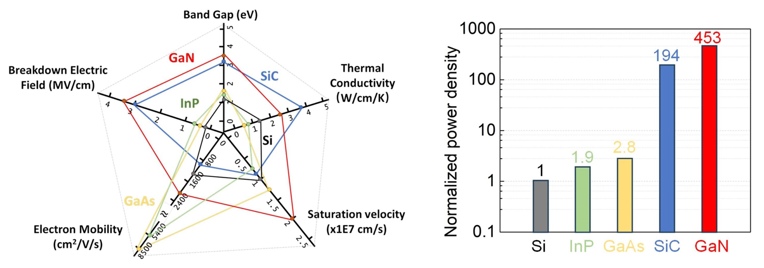
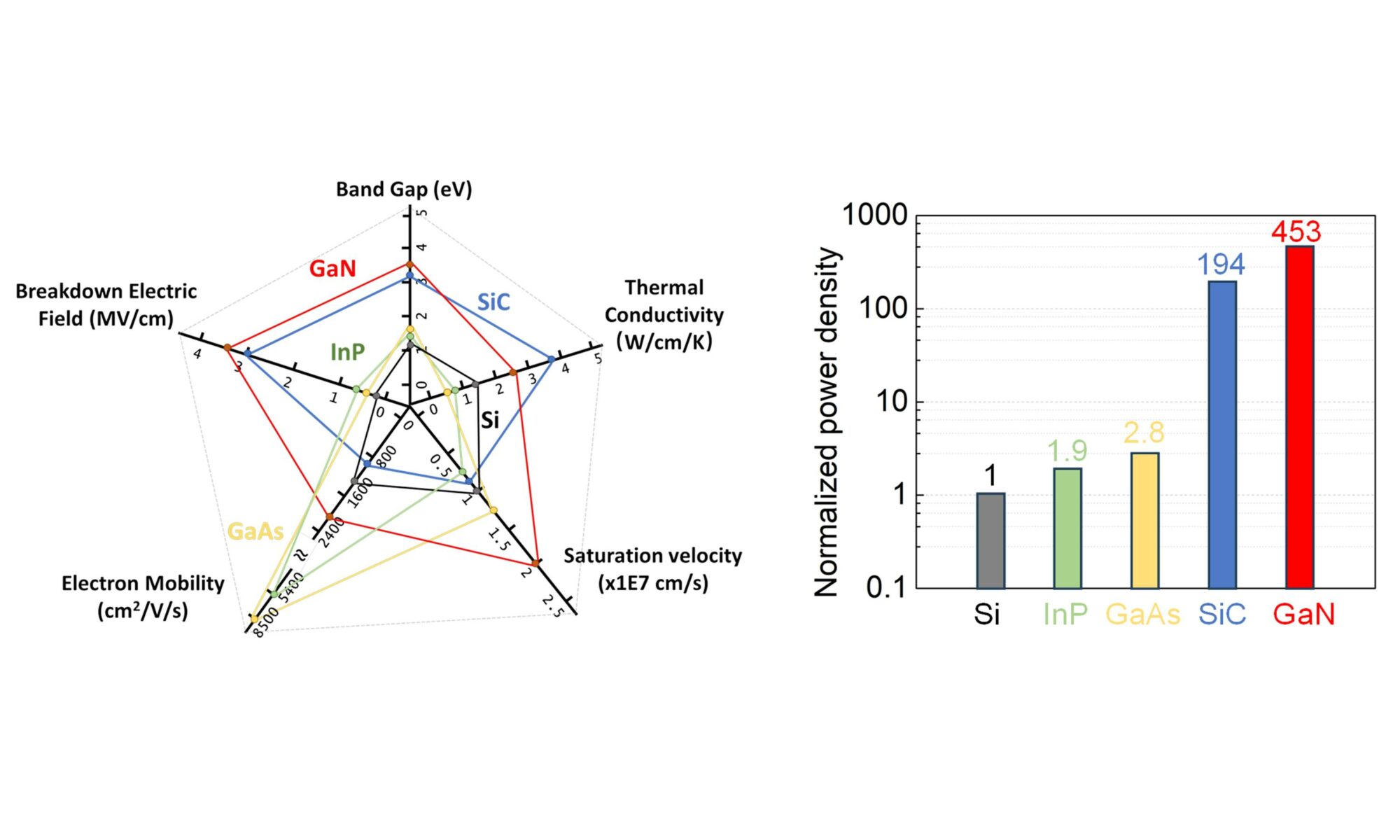
Gallium nitride (GaN) proves its prominence in high-power high-frequency RF applications due to its superior properties, such as high critical field, high mobility, and high saturation velocity. These merits make GaN a prime candidate for making IMPATT diodes, which promise to offer the best power-frequency performance among solid-state semiconductor RF devices. Theoretical analysis predicts GaN IMPATT diodes can offer a power-frequency product 450 times higher than their silicon counterparts. However, the experimental demonstration of GaN IMPATT diodes has been long hindered by the absence of achieving uniform avalanche. In 2020, an 800 MHz oscillation was observed for the first time in a GaN pn diode, capable of avalanche breakdown. The latest results presented by Stanford University at 2024 IEDM significantly advanced GaN IMPATT technology, reaching 60 GHz oscillation.
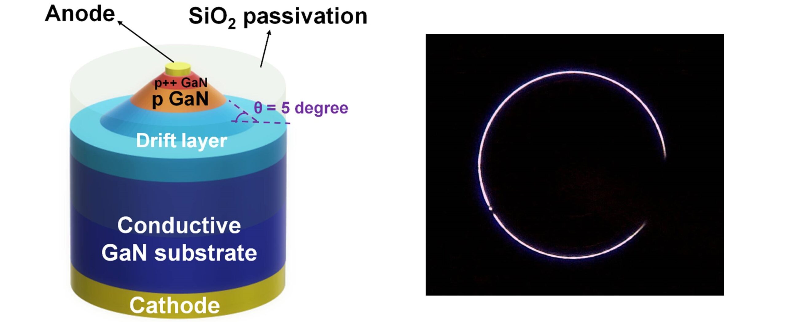
IMPATT diodes are such unique devices that they operate in the breakdown regime. For GaN, edge termination structures are vital to prevent field crowding and premature device breakdown. In this work, a 5-degree bevel mesa etch was utilized to ensure a uniform avalanche, verified by the uniform electroluminescence in the device during the unclamped inductive switching test.

It’s worth emphasizing that developing high-performance IMPATT diodes requires much more than just meeting the avalanche requirement. It’s equally important to reduce the parasitic resistance to achieve efficient high-frequency operation and enhance heat dissipation to improve power density and device reliability. To address the above two challenges, the Stanford team, in collaboration with QuinStar Technologies Inc., developed a bulk GaN substrate thinning process and packaged the diode with the integration of a type IIa diamond heat sink.
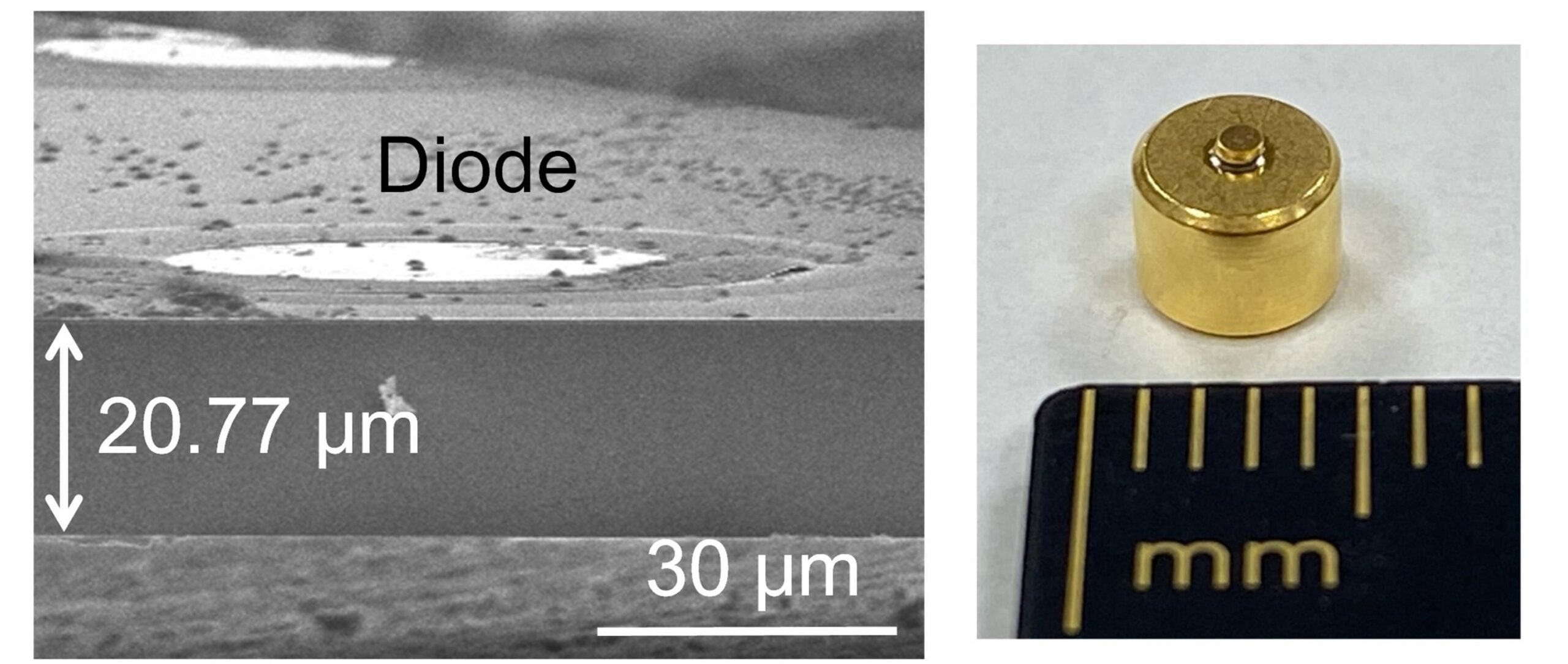
The thinning process was carefully optimized to thin down bulk GaN substrate from 400 to 20 µm while keeping the avalanche capability in the diodes intact. The total on-resistance was reduced by 54 %, the leakage current remained minimal, and the breakdown voltage was maintained the same after the thinning process.
A specially designed ceramic pill with the integration of a diamond heat sink as the base was utilized to package the diode. This package offered minimal parasitic elements up to W-band operation. The adoption of a diamond heat sink supported the diode to sustain a high input power density of 2.65 MW/cm2 without burn-out.

The packaged diode was embedded in a waveguide resonant cavity and tested using an industry testbed at QuinStar Inc. The oscillator circuit featured a sliding backshort for impedance tuning. At a biasing current of 17.1 kA/cm2, the diode was capable of delivering a 60.8 GHz oscillation with 12.7 dBm power. This result marks the first GaN IMPATT oscillator reaching V-band operation, showcasing its great potential for mm-wave applications.
RF oscillation characteristics of the GaN IMPATT oscillator and performance benchmark
Looking ahead, there remains significant potential for improvement. Currently, the GaN substrate is the primary contributor to thermal resistance. To overcome this limitation, achieving a flip-chip configuration and enhancing the thermal boundary conductance between the GaN and diamond interface are critical for increasing the thermal capacity of GaN IMPATT diodes. Device-to-circuit co-optimization is another key to boosting the system efficiency and output power. Our next steps will center on electro-thermal co-design to fully unlock GaN’s potential for next-generation IMPATT technology.
The Presenter
Stanford University and QuinStar Technologies Inc. Under the leadership of Prof. Srabanti Chowdhury, the Wide-Bandgap Lab at Stanford has been at the forefront of GaN vertical device innovation. Their recent work on diamond and GaN integration for advanced thermal management has garnered significant attention for pushing performance boundaries.
The IMPATT devices, a core focus of Zhengliang Bian’s research, a Ph.D. student under Prof. Chowdhury, were a central part of this work who presented it at the IEDM this year. Avery Marshall led the circuit design and measurements, working closely with Lissete Zhang and Tracey Lee. Key innovations in edge termination, wafer thinning, heat sinking, and uniquely designed packaging enabled the successful demonstration of this technology, paving the way for a promising roadmap in this field.
Also Read:
Intel Presents the Final Frontier of Transistor Architecture at IEDM
TSMC Unveils the World’s Most Advanced Logic Technology at IEDM
IEDM Opens with a Big Picture Keynote from TSMC’s Yuh-Jier Mii
Share this post via:


Chemical Origins of Environmental Modifications to MOR Lithographic Chemistry