
- This event has passed.
Wafer Fab Processing
November 25, 2024 - November 28, 2024

Semiconductor and integrated circuit developments continue to proceed at an incredible pace. The industry as a whole has gotten to this point of incredible complexity through the process of countless breakthroughs and developments in wafer fab processing. Today’s wafer fab contains some of the most complex and intricate procedures ever developed by mankind. Wafer Fab Processing is a 4-day course that offers an in-depth look into the semiconductor manufacturing process, and the individual processing technologies required to make them. We place special emphasis on the basics surrounding each technique, and we delve into the current issues related to manufacturing the next generation devices. This course is a must for every manager, engineer and technician working in the semiconductor industry, using semiconductor components or supplying tools to the industry.
By focusing on the basics of each processing step and the issues surrounding them, participants will learn why certain techniques are preferred over others. Our instructors work hard to explain how semiconductor processing works without delving heavily into the complex physics and mathematical expressions that normally accompany this discipline.
What Will I Learn By Taking This Class?
Participants will learn basic, but powerful, aspects about the semiconductor industry. This skill-building series is divided into three segments:
- Basic Semiconductor Wafer Processing Steps. Each processing step addresses a specific need in IC creation. Participants will learn the fundamentals of each processing step and why they are used in the industry today.
- The Evolution of Each Processing Step. It is important to understand how wafer fab processing came to the point where it is today. Participants will learn how each technique has evolved for use in previous and current generation ICs.
- Current Issues in Wafer Fab Processing. Participants will learn how many processing steps are increasingly constrained by physics and materials science. They will also learn about the impact of using new materials in the fabrication process, and how those materials may create problems for the manufacturers in the future.
This course is a must for every manager, engineer, and technician working in the semiconductor industry, using semiconductor components, or supplying tools to the industry. Our instructors work hard to explain how semiconductor wafer processing works without delving heavily into the complex physics and mathematical expressions that normally accompany this discipline.
Course Objectives
- The course will provide participants with an in-depth understanding of the semiconductor industry and its technical issues.
- Participants will understand the basic concepts behind the fundamental wafer fab processing steps.
- The course will identify the key issues related to each of the processing techniques, and their impact on the continued scaling of the semiconductor industry.
- The course offers a wide variety of sample problems that participants will work to help them gain knowledge of the fundamentals of wafer fab processing.
- Participants will be able to identify the basic features and principles associated with each major processing step. These include processes like chemical vapor deposition, ion implantation, lithography, and etching.
- Participants will understand how processing, reliability, power consumption and device performance are interrelated.
- Participants will be able to make decisions about how to construct and evaluate processing steps for CMOS, BiCMOS, and bipolar technologies.
Course Outline
Day 1
- Basics and Fundamentals: Semiconductor Devices and ICs
- Acronyms
- Common Terminology
- Brief History
- Semiconductor Materials
- Electrical Conductivity
- Semiconductor Devices
- Classification of ICs and IC Processes
- Integrated Circuit Types
- Crystallinity, Crystal Defects, Crystal Growth
- Crystallinity
- Crystal Defects
- Crystal Growth
- Controlling Crystal Defects
- Basic CMOS Process Flow
- Transistors and Isolation
- Contacts/Vias Formation
- Interconnects
- Parametric Testing
- Ion Implantation 1 (The Science)
- Doping Basics
- Ion Implantation Basics
- Dopant Profiles
- Crystal Damage and Annealing
- Ion Implantation 2 (Equipment, Process Issues)
- Equipment
- Process Challenges
- Process Monitoring and Characterization
- New Techniques
Day 2
- Thermal Processing
- Overview of Thermal Processing
- Process Applications of SiO2
- Thermal Oxidation
- Thermal Oxidation Reaction Kinetics
- Oxide Quality
- Atomistic Models of Thermal Diffusion
- Thermal Diffusion Kinetics
- Thermal Annealing
- Thermal Processing Hardware
- Process Control
- Contamination Monitoring and Control
- Contamination Forms and Effects
- Contamination Sources and Control
- Contamination Characterization and Measurement
- Wafer Cleaning
- Wafer Cleaning Strategies
- Chemical Cleaning
- Mechanical Cleaning
- Vacuum, Thin Film, and Plasma Basics
- Vacuum Basics
- Thin Film Basics
- Plasma Basics
- Chemical Vapor Deposition 1 (Basics, LPCVD, Epitaxy)
- CVD Basics
- LPCVD Films
- LPCVD Equipment
- Epi Basics
- Epi Process Applications
- Epi Deposition Process
- Epi Deposition Equipment
Day 3
- Physical Vapor Deposition
- PVD Basics
- Sputter Deposition Process
- Sputter Deposition Equipment
- Al-Based Films
- Step Coverage and Contact/Via Hole Filling
- Metal Film Evaluation
- Lithography 1 (Photoresist Processing)
- Basic Lithography Process
- Photoresist Materials
- Photoresist Process Flow
- Photoresist Processing Systems
- Lithography 2 (Image Formation)
- Basic Optics
- Imaging
- Equipment Overview
- Actinic Illumination
- Exposure Tools
- Lithography 3 (Registration, Photomasks, RETs)
- Registration
- Photomasks
- Resolution Enhancement Techniques
- The Evolution of Optical Lithography
- Etch 1 (Basics, Wet Etch, Dry Etch)
- Etch Basics
- Etch Terminology
- Wet Etch Overview
- Wet Etch Chemistries
- Types of Dry Etch Processes
- Physics and Chemistry of Plasma Etching
Day 4
- Etch 2 (Dry Etch Applications and Equipment)
- Dry Etch Applications
- SiO2
- Polysilicon
- Al and Al Alloys
- Photoresist Strip
- Silicon Nitride
- Dry Etch Equipment
- Batch Etchers
- Single Wafer Etchers
- Endpoint Detection
- Wafer Chucks
- Chemical Vapor Deposition 2 (PECVD)
- CVD Basics
- PECVD Equipment
- CVD Films
- Step Coverage
- Chemical Mechanical Polishing
- Planarization Basics
- CMP Basics
- CMP Processes
- Process Challenges
- Equipment
- Process Control
- Copper Interconnect, Low-k Dielectrics
- Limitations of “Conventional” Interconnect
- Copper Interconnect
- Cu Electroplating
- Damascene Structures
- Low-k IMDs
- Cleaning Cu and low-k IMDs
- Leading Edge Technologies and Techniques
- Process Evolution
- Atomic Layer Deposition (ALD)
- High-k Gate and Capacitor Dielectrics
- Ni Silicide Contacts
- Metal Gates
- Silicon on Insulator (SOI) Technology
- Strained Silicon
- Hard Mask Trim Etch
- New Doping Techniques
- New Annealing Techniques
- Other New Techniques
- Summary of Industry Trends
Instructional Strategy
Our courses are dynamic. We use a combination of instruction by lecture, problem solving, and question/answer sessions to give you the tools you need to excel. From the very first moments of the seminar until the last sentence of the training, the driving instructional factor is application. The course notes offer hundreds of pages of reference material that you can apply during your daily activities. Additionally, the opportunity to work through sample problems under the guidance of an expert instructor allows you to cement the concepts you learn through hands-on implementation.
Our instructors are internationally recognized experts. Our instructors have years of current and relevant experience in their fields. They’re focused on answering your questions and teaching you what you need to know.
Instructor Profile
Jim Fraser
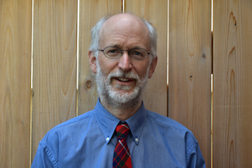
Jim Fraser received a Bachelor’s degree in Physics from McGill University in Montreal, Quebec, Canada. He has many years experience in semiconductor manufacturing, at Nortel Networks and STMicroelectronics. As a Process Engineer, Process Engineering Section Manager, and then Process/Device Engineering Manager, he worked directly and intimately with CMOS and BiCMOS wafer fab processes. He has taught semiconductor manufacturing technology at Algonquin College and at the University of Ottawa in Ottawa, Ontario, and has guest lectured at McGill University. More recently he has provided process analysis services on contract to Chipworks (now TechInsights) in Ottawa.






IEDM 2025 – TSMC 2nm Process Disclosure – How Does it Measure Up?