 At TSMC’s OIP Symposium last month, Zhe (Jared) Lui of HiSilicon presented their experiences with Synopsys’ ICC2 physical design suite.
Jared started by giving an overview of Huawei and HiSilicon. HiSilicon is the semiconductor arm of Huawei. I assume everyone knows who Huawei is. To a first approximation they are the Cisco of China, although they are also in consumer facing businesses. In particular, they are currently (Q2) #3 in worldwide smartphone market share (ahead of Xioami and Lenovo/Motorola). They are the largest telecommunication manufacturer in the world, having passed Sweden’s Ericsson a couple of years ago.
I was surprised to find that HiSilicon started in 1991. They are the #1 fabless company in China, with over 5500 employees. They are headquartered in Shenzhen (just across a river from Hong Kong if you are unsure where that is) but have over 20 R&D centers in 10 countries and regions. If you have driven down Central expressway where it goes over San Tomas expressway you have seen their Silicon Valley campus.
Their current production smartphone chips are in TSMC 28nm HPC. For example, the Kirin 935 application processor for the Huawei P8 MAX was created by HiSilicon. It contains an 8 core big-LITTLE ARM Cortex A53e/A53, runs at either 2.2GHz or 1.5GHz, has an ARM Mali 628 GPU. It has a dual SIM LTE Cat 6 modem (300Mb/s downlink, 50Mb/s uplink).
In networking they are already at 16nm. In fact their 32-core ARM Cortex-A57 networking chip was the world’s first 16nm production tapeout at TSMC using Synopsys physical design (in March of this year). Each ARM CPU is 1.6M instances with 78 macros (and there are 32 of them) so this is a big chip.
Jared then talked about the main implementation challenges at advanced nodes:
- colored flow for advanced patterning
- vertical placement constraints to to enable pin accessibility on ever shrinking standard cell layouts
- highly heterogeneous metal stacks (low levels metals have high resistance)
- increasing electromigration issues due to high switching activity and high power draw
- on-chip variation and the need for increased accuracy, parametric OCV
- timing accuracy in the multi-patterned world, and low voltage delay effects
Synopsys introduced IC Compiler II (ICC2) in March of 2014 with a promise of 10X increased throughput and productivity compared to what is just called IC Compiler (but I’ll call it ICC1 to be clearer). The promise of the same or better results faster interested HiSilicon, thus initiating a close working partnership to see if ICC2 could deliver on that promise. HiSilicon and Synopsys initiated a partnership in 3 phases.
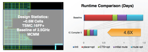
Phase 1, full P&R on complex, high performance CPU blocks. On a design with about 600K cells in TSMC 16FF+ with 2.5GHz clock, multi-mode multi-corner timing IC2 then ICC2 reduced run time from 1.5 days to 0.3 days meaning multiple iterations per day. This is a speedup of 4.6X.

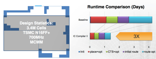
Phase 2, full P&R on high capacity blocks from GPU designs. On a design with 3.4M cells in TSMC 16FF+, 700MHz, MCMM, the speedup was 3X from over 4 days to less than 1.5 days.

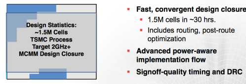
Phase 3, P&R of latest node silicon validation vehicle. 1.5M cells, a TSMC process (unnamed, but I’m guessing 10nm), 2GHz+, MCMM, power-aware flow. Result was a run time of about 30 hours delivering signoff quality timing and DRC.

Some of the key features of ICC2 that contributed to HiSilicon’s success:
- advanced timing analysis: accurate timing at advanced nodes and low voltage
- automatic clock layer optimization: use low resistance metal layers for long nets
- post-route clock closure
- power reduction with DesignWare and DC Ultra for datapaths
- advanced power recovery in PrimeTime: downsizing cells on positive slack paths, Vt cell swaps for power recovery
The end of the story is that ICC2 delivered 3-5 times runtime benefit while using less than half the memory, and delivering better QoR out-of-the-box. The reduction of design iterations further shortened development time. HiSilicon have decided to deploy ICC2 in production for new node design work, and are also expanding their collaboration with Synopsys and TSMC going forward.
If you attended OIP, even if you didn’t attend this session, the slides are in the handout book. Or you can get more information on ICC2 HERE.
Share this post via:


Comments
0 Replies to “HiSilicon’s Experience with Synopsys ICC2”
You must register or log in to view/post comments.