Every industry has famous thought leaders that can summarize where we’ve been and then paint a picture of where we’re headed towards in the future. Often they make statements that become industry expressions, like “Moore’s Law” or the “Internet of Things”. I think that if Synopsys Chairman Aart de Geus had his way, then history would remember him for the phrase, “Techonomics”. At the annual SNUG meeting last month Mr. de Geus spoke about, “Design Change Into Semiconductor Techonomics”, and I watched the 65 minute video recording to better understand his industry vision.
Innovation is not dead, technology and economics (techonomics) have Moore’s law growing for another 10 years. From the business side you can look at our technology industries by market size:
- Applications – $Zillions (Mobile $79B, PC/Server $72B, Auto $20B)
- Electronics $1.4T
- Semiconductor $300B
- EDA + IP $7B
- Fabrication $40B.
How is the semiconductor industry doing? Still growing, about 4.7% CAGR now, however there have been years of wild swings caused by the global economy and supply/demand discontinuities.
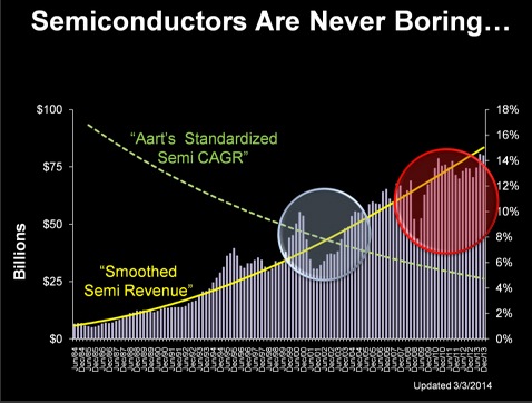
Business demands for growth then create pressure to design electronic products that are sooner, better and cheaper while being different from competitors. The Smart Phone market has been driven largely by sooner and better suppliers, while for emerging geographies the emphasis instead is on cheaper.
Looking at the history of transistor nodes used by Synopsys customers there is a rhythm to how fast they are adopted and ramped up. The following chart shows the tape out ramp history for 90nm node in purple, 65nm node in green, 45/40nm node in blue, and the 32/28nm node in red.
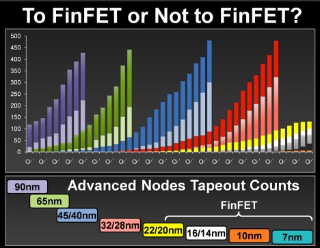
The node plans down to 7nm are well understood per conversations with Dr. Bohr at Intel. FinFET technology has started at the 22/20nm nodes and lower.
Synopsys has been offering design software, semiconductor IP and verification tools, which span up to prototyping and down to manufacturing. Improvements to design software include IC Compiler II (blogged by Paul McLellan, and myself) with a 10X improvement goal in speed, capacity and QOR. About ST using IC Compiler II, Aart said, “At 28nm an FD-SOI chip, very interesting technology, holding high promise for low power at a reasonable cost.”
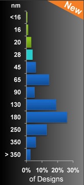
An interesting plot was the popularity of process nodes on a range of designs done by Synopsys customers because the majority of designers are at 180nm, not the bleeding edge:
You can even take a design implemented with a mature 130nm node and route it with fewer layers and get a smaller area using IC Compiler II. Re-working the Synopsys tools even sped up the simulation times between VCS (digital) and SPICE (analog) by 6X. On the functional verification side of EDA, Aart talked about how Verification Compiler is comprised of their tools for debug, static and formal, simulation, verification IP, plus coverage and planning (blogged by Paul McLellan). As Synopsys has acquired point-tool companies, then it takes time to make the integrations native which then provides speed ups and capacity improvements.
IoT has now been branded as smart everything by Aart. The growth rate of sensors is rapid at a 30% CAGR, like in automotive applications.
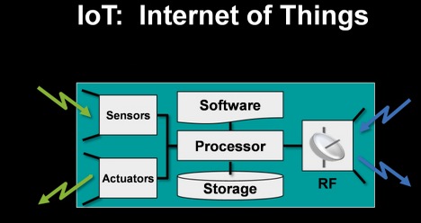
To serve this IoT market, Synopsys has created a sensor IP subsystem to include both software and IP to work with the most popular host interfaces, sensors and actuators. IP must work in the most popular process nodes and support standards like USB 3.1, DDR4 and 12G enterprise PHY. IP re-use enables the faster time to market requirements of IoT designs.
Prototyping a new system with models for both hardware and software is a continuing challenge, and Synopsys engineers just wrote a free book called Better Software, Faster!, about best practices in virtual prototyping.
Some 50% of engineers at semiconductor companies are now software engineers, not hardware engineers – so Synopsys is looking to enter that market by the acquisition of Coverity to enable: code analysis, test analysis, metrics and measurement, workflow and collaboration. It’s a bold move, way outside the comfort zone in traditional EDA companies.
Summary
The success of semiconductor, EDA, IP, embedded and software industries are highly interdependent, just like the gears in a machine. Collaboration is essential for continued success.
lang: en_US
Share this post via:


Comments
There are no comments yet.
You must register or log in to view/post comments.