
By Todd Burkholder and Per Viklund, Siemens EDA
The landscape of advanced IC packaging is rapidly evolving, driven by the imperative to support innovation on increasingly complex and high-capacity products. The broad industry trend toward heterogeneous integration of diverse die and chiplets into advanced semiconductor package systems has led to an explosion in device complexity and pin counts.
Thus, the adoption of chiplets is accelerating at an unprecedented pace. Chiplets offer a modular solution, providing smaller, convenient building blocks that communicate via standardized interfaces, thereby enabling more flexible and cost-effective system integration.
The complexity of packages themselves is experiencing explosive growth. Package pin counts have surged from approximately 100,000 or fewer pins just a few years ago to upwards of 50 million pins in contemporary designs. Projections indicate a potential tenfold increase in these numbers within the next few years, creating a profound impact across every facet of the semiconductor ecosystem.
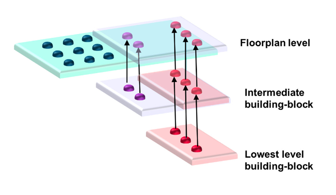
The sheer scale of this complexity far exceeds the capacity of any single human designer to manage effectively. A solution capable of abstracting this complexity into manageable portions is indispensable. This is precisely where hierarchical device planning becomes paramount. It represents a methodology and a suite of technologies designed to decompose overwhelming complexity into digestible, manageable segments.
A salient significant challenge lies in optimizing smaller functional areas within a package and subsequently reusing these optimized blocks in derivative designs. Hierarchical device planning directly addresses this by integrating established hierarchical design methodology techniques—long characteristic of chip design—into the realm of advanced IC packaging. This approach is crucial for managing the intricate interface connectivity inherent in package devices composed of numerous smaller building blocks.
However, before fully embracing a hierarchical design implementation strategy, it is crucial to acknowledge the unique challenges of IC packaging. A key challenge is that, at the top level, hierarchical floorplans require a unique set of signals for each instance of a placed building block.
Out with the old, in with the new
Designing viable bump patterns for chiplets and interposers involves managing a multitude of signals, interface I/Os, and power and ground connections. While managing perhaps 100,000 pins, as was common some years ago, was challenging but generally feasible, albeit prone to errors, the current reality of millions or even 50 million pins renders such manual approaches absolutely unworkable. Consequently, traditional assembly and planning methodologies, which model large-capacity pin devices like high-performance computing die as single, flat entities, are no longer sufficient. These flat approaches demand extraordinary designer skill to manage the connectivity and topological relationships of all functional blocks.
For packaging designs of lower complexity, and even sometimes for reasonably complex current designs, the traditional tool of choice has often been spreadsheets, particularly Microsoft Excel. While spreadsheets may suffice for small designs, they become woefully inadequate when dealing with multiple chiplets, their intricate interfaces, and the presence of interposers or silicon bridges. Furthermore, in many advanced packaging scenarios, some components are co-designed concurrently with the package itself, meaning they are in a constant state of flux. The sheer volume of data and the imperative to maintain synchronization across all these dynamic elements make these manual methods entirely unviable.
The consequences of errors in package assembly can be catastrophic. Historically, there have been instances where such errors have led to astronomical financial repercussions, even resulting in the demise of entire companies. The costs associated with a failed package, especially a large, complex one, are immense. The long-term consequence, assuming a company survives such a setback, is an invaluable—albeit painful—lesson learned, driving a commitment to never repeat the mistake. This underscores the critical need for robust, error-preventing methodologies and tools from the outset.
Modern advanced packaging demands solutions capable of managing the entire package assembly as a unified entity. This includes robust capabilities for tracking connectivity throughout the complete package assembly and providing comprehensive, full-package assembly verification in three dimensions. Given that all these advanced packages inherently involve some form of 3D integration, validating their structural and electrical integrity is paramount. It is crucial to remember that a package now comprises multiple designs stacked together—chiplets, interposers, silicon bridges, and other elements. Relying on traditional, disconnected methods for such complex assemblies introduces an unacceptably high risk of failure. This necessitates a transition to a more synchronized and integrated design methodology.
A new paradigm for managing IC complexity
This is precisely where hierarchical device planning introduces a new paradigm. The core innovation lies in the ability to hierarchically define parameterized regions of component pins. Instead of grappling with the minutiae of every single pin and its connectivity, designers can now work with these abstracted, hierarchically defined regions. This allows them to plan, design, analyze, and optimize the overall package layout at a higher level of abstraction, deferring the detailed pin-level considerations until they are genuinely necessary.
A significant advantage of this approach is the automatic synthesis of all pins according to the parameters set within these defined regions. Package designers are intimately familiar with the frequent design changes that occur throughout the development flow. Traditionally, implementing each change individually was a time-consuming and error-prone process. With hierarchical device planning, designers can simply modify the relevant parameters of a region, and the system automatically updates the circuit. This capability can save days, or even weeks, of design effort, representing a critical leap in efficiency and responsiveness to design iterations.

Enabling 3D IC solutions
The trajectory of IC packaging development mandates the adoption of appropriate methodologies and tools that directly address the designer’s evolving challenges. Foremost among these is the need to shield designers from being overstretched by complexity, a common outcome when tools fail to provide adequate support. Designers require assistance to operate at a practical abstraction level—one that renders the design manageable. Presenting a designer with 50 million pins without context offers no actionable insight into optimizing the design. Instead, tools must facilitate a higher-level view that guides optimal design decisions.
Furthermore, these solutions must provide access to multi-domain analysis very early in the design cycle. This includes critical analyses such as signal integrity (SI), power integrity (PI), thermal analysis, and thermal stress analysis. Performing these analyses proactively, long before the package layout is finalized, is essential for driving early design decisions and ensuring the correct path is taken when choices arise. Discovering major issues post-layout is extraordinarily costly, often necessitating a complete package redesign—a luxury rarely afforded by tight development schedules. Early analysis is therefore indispensable.
Siemens’ Innovator 3D IC portfolio solution exemplifies this integrated approach, supporting designers from initial planning and optimization through detailed analysis and package layout.

A critical component of this solution is robust work-in-progress data management. The sheer volume of data involved in a modern package design demands meticulous tracking to ensure the correct versions of all files are utilized. Forgetting to import an updated Verilog file, for instance, can lead to the fabrication of an incorrect package. Automated tracking and error detection mechanisms are vital to mitigate the numerous potential points of failure. By integrating these capabilities within a unified, AI-infused user experience, solutions like the Innovator 3D IC solution suite are intuitive and efficient for designers to adopt and utilize.
Package designers must leverage every available tool to address the significant device complexity and the explosion in pin counts characteristic of today’s IC packaging designs. In support of this, a concerted effort is underway to develop new solutions, standards, and methodologies. For instance, new interface standards, such as UCI Express, Bunch of Wires (BOW), and Advanced Interface Specification (AIS), are emerging to standardize communication between chiplets. Concurrently, advanced design methodologies and tools are being developed to assist design teams and facilitate seamless interaction with foundries, substrate fabricators, and OSAT providers.
It is crucial for all professionals involved in package design to recognize that effective solutions are available. While many designers may perceive their specific challenges as unique, in most cases the underlying problems are shared across the industry. Fortunately, this leads to a common set of solutions. By actively seeking out and adopting these advanced tools and methodologies, designers can more effectively tackle the complexities of 3D ICs and heterogeneous integration, ensuring the successful realization of next-generation electronic systems.
Also Read:
A Compelling Differentiator in OEM Product Design
AI-Driven DRC Productivity Optimization: Revolutionizing Semiconductor Design
Visualizing hidden parasitic effects in advanced IC design
Share this post via:


Comments
There are no comments yet.
You must register or log in to view/post comments.