Monday at DAC this year started off on a very optimistic note as Joe Sawicki from Siemens EDA presented in the Pavilion on the topic of Digitalization, a frequent theme in the popular press because of the whole Work From Home transition that we’ve gone through during the pandemic. Several industries are benefiting from the digitalization trend: semiconductor, aerospace, defense, automotive, heavy machinery, medical, consumer products, energy, utilities and even marine.
The ever-present Tesla leads the way in EV sales as owners enjoy the benefits of SW updates over the air, adding new features and fixing bugs, much like our smart phone apps, all enabled by semiconductors. Even President Biden extols the virtues of semiconductor production in the US, and how national policy should benefit the semiconductor industry.
During the pandemic we’ve experienced trauma because of illness and death, yet the move to digital commerce has sharply risen, and cloud-based services are flourishing, like Zoom and Microsoft Teams. Most modern businesses are quickly moving their services and support to digital and cloud platforms.
Semiconductor content in electronic products has moved from 16% up to 25% as a mega-trend, think: Amazon, Google, Tesla, Bosch, ZTE, Huawei, Apple and Facebook.
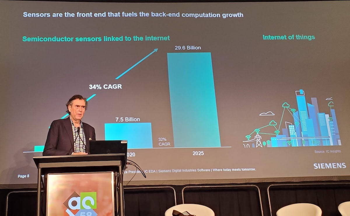
Foundry revenue trends are showing that systems companies are growing at a 26.8% CAGR, which is a big shift in who does SoC designs. Some of the drivers at foundries include: Sensors, edge computing, 5G, wireless, cloud and data center. Just in the past 5 years there has been a 5X increase in the number of sensors connected to the Internet, projected to reach 29.6 billion devices by 2025. An example of connected sensors is the Ring Doorbell.
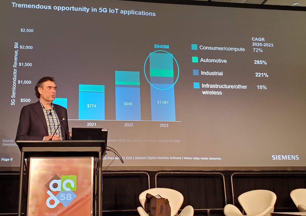
There’s growth in how 5G and IoT markets are linked, and even data centers are forecasted to have a 14% CAGR during the 2028-2030 period. The flow of information is from sensors, to edge processing, to 5G or wireless, and it is all ending up in a data center.
Within the next 10 years the projection is that 95% of our vehicles will be connected, which creates big demands on the wireless infrastructure. ADAS is expected to have a 22% CAGR from 2020 to 2030. The value of Electronic Control Units (ECUs) in a car went from $302 in 2010, to $499 in 2020, and is expected to reach $758 by 2030. The electrification trend in automotive is in growth mode, so one challenge is to hire enough system designers to keep pace with competitive demands.
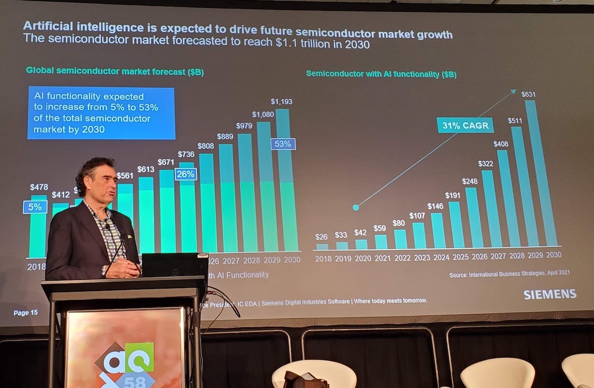
AI in semiconductor has a steep growth of some 31% CAGR to 2030, and it’s becoming a pervasive technology. We now have chips optimized for AI training and inferencing. Semiconductor companies are starting new domain-specific AI chips in diverse areas like: voice, video, cyber security, IoT, odor detection, etc.
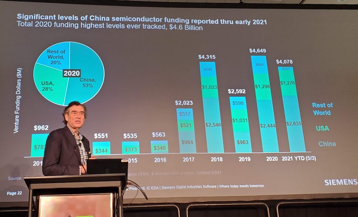
The overall semiconductor revenues are predicted to grow at a 9.5% CAGR over 2020-2025, while the GDP CAGR is a bit lower at 6.2%, so let the good times continue to roll. Even the US government is considering legislation to fund research in the semiconductor industry to help gain critical market share. Even VC funding for fabless companies reached some $8B in 2021, setting another world record year. Foundry investments are expected to reach $79.6B in 2021.
Historically the R&D funding as a percentage of revenue for semiconductor companies has been about 14.2%, while it has ranged from 12% to 18% over the years. During the pandemic our industry has seen shortages in the supply chain, as demand is strong, however the basic materials can be scarce. The shortage is slowing down our consumer and industrial productivity, but how much double ordering is really going on right now?
The majority of VC investing in semiconductor has focused on China markets recently, at 53%.
In our EDA world the revenues are driven by new design starts, not semiconductor revenues, so just how many new designs will start using the 5nm node? We’ve seen failed predictions in the past, like some who said that only 3 companies would even attempt a 5nm design. In reality, IC design starts are quite strong in many areas: wearables, IoT, ADAS, industrial, smart grid, 5G. In Q2 of 2021 the EDA revenues were at $3B, a growth of 14.6%, so that’s a healthy increase, and EDA has seen four quarters now of double-digit growth. In fact, EDA revenues have recently seen their highest growth rate in the past 10 years.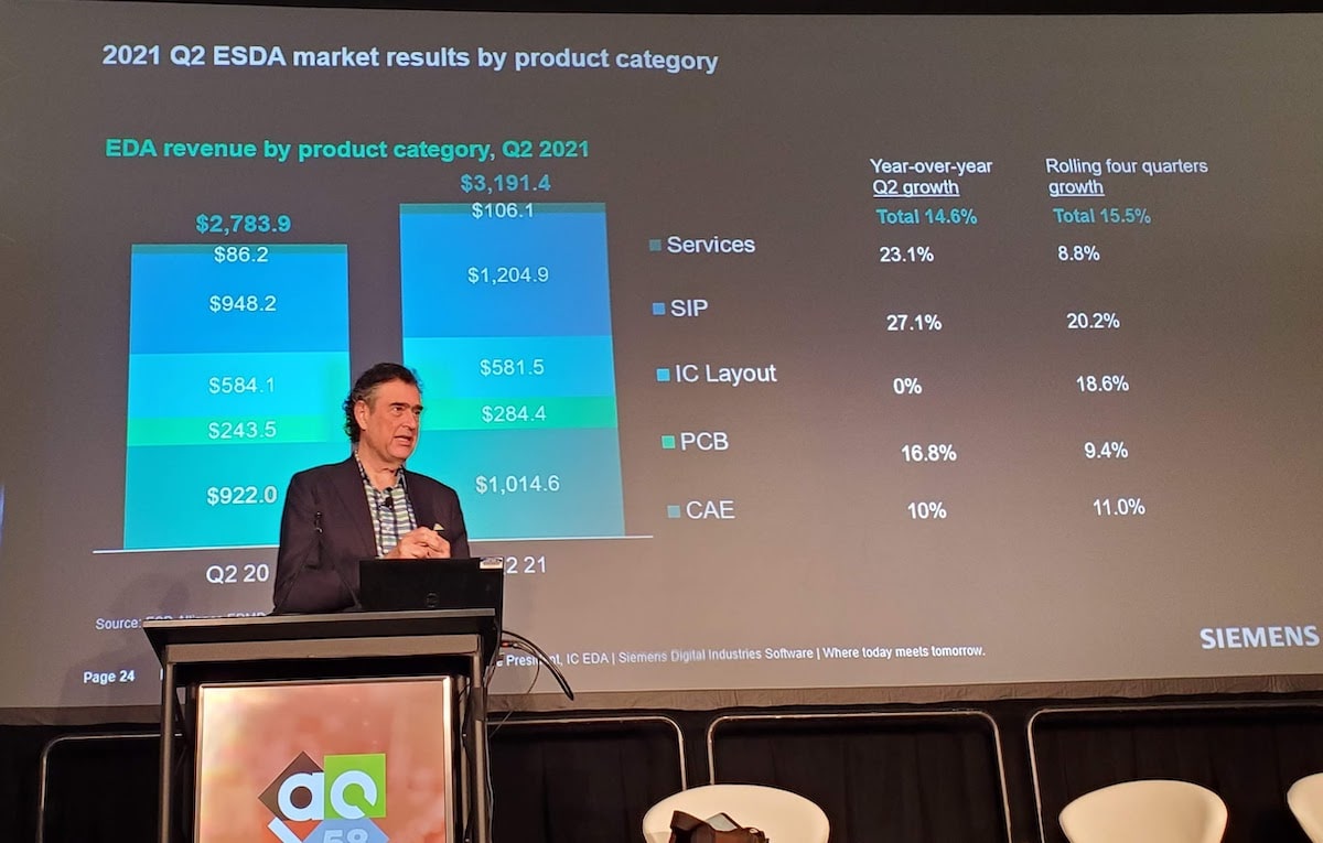
Diving a bit deeper, the following areas are driving EDA growth:
- AMS, RF – 12.4%
- DFT – 9.7%
- IC Full Custom – 8.4%
- Formal – 8.4%
- Logic – 7.4%
- Layout Verification – 7.4%
- P&R – 7%
- PCB – 10%
Challenges going forward into the next decade include three areas: Technology scaling, Design scaling, System scaling. Looking at Apple as an example of a systems company designing their own A-series of processors over the past 8 years, where the A7 processor had about 1 billion transistors, while the latest A15 processor includes some 15 billion transistors, almost in perfect alignment with a 16X increase predicted by Moore’s Law.
Machine learning as a technique is being applied to EDA tools to enable accelerations in yield ramp, pattern analytics, and metrology. Predicted costs for design scaling are that 3nm SoC costs could range from $535M – $626M. In EDA the use of High Level Synthesis (HLS) continues, and Siemens has offered HLS for about 25 years now. With HLS systems companies like NVIDIA are designing new chips with a small group of just 10 engineers in just 6 months. As AI techniques become more ubiquitous, we can expect to see even more accelerator products announced that are application specific, and during the design phase the engineers will explore to find the optimum architecture.
Another new acronym is STCO, short for System Technology Co-Optimization, where multiple die and chiplets are being used to assemble new systems, along with the use of 3D die stacking, and other advanced packaging concepts.
For system scaling the path forward calls for mixed-mode, virtual simulations, along with hardware-assisted verification techniques like using emulation, where a systems designer can actually run real apps even before the silicon has been manufactured. Emulation will also be used more for the debug of HW/SW integration issues early in the design process.
Within Siemens there’s something called PAVE360, that allows a systems approach to model, sense, compute, analyze and actuate as a model, prior to implementation. In the pursuit of autonomous vehicles, using a PAVE 360 methodology is more practical than driving billions of actual miles to uncover safety issues.
Summary
Mr. Sawicki was quite upbeat about the semiconductor industry trends, and the number of IC design starts is great news for EDA vendors of all types, although there are formidable challenges ahead to meet the scaling demands.
Also Read:
System Technology Co-Optimization (STCO)
Siemens EDA will be returning to DAC this year as a Platinum Sponsor.
Machine Learning Applied to IP Validation, Running on AWS Graviton2
Share this post via:



Comments
There are no comments yet.
You must register or log in to view/post comments.