In January I read from the ESDA Allianceabout EDA and Semiconductor IP revenues increasing 6.7% for Q3 2018, reaching $2,435.6 million, which is decent growth for our maturing industry. In stark contrast there’s a company called Methodicsthat specializes in Intellectual Property Lifecycle Management (IPLM) and traceability that has a much higher growth rate than the industry average. To get better informed I spent some time asking questions of two contacts at Methodics: Jerry Brocklehurst, VP of Marketing and Simon Butler, President and CEO.

Jerry Brocklehurst, Simon Butler
Q&A
Q: I know that you’re still a privately held company and don’t publish a detailed quarterly financial report, but what can you tell me about your growth rate?
Jerry: Well, we just reported 5 consecutive years of greater than 50% growth rate per year from 2014 through 2018.
Q: Wow, a 50% growth rate is way above the industry average. What trends are happening in the semiconductor industry that account for such rapid adoption of your IPLM tools?
Jerry: Over the past 5 years, semiconductor companies have found it mission-critical to implement design reuse strategies across their organizations in order to meet time-to-market, financial, and profitability goals while also facing tougher competition to design and produce ever more complex designs.
As design elements and IPs are being reused in different chips, a further challenge is the need to track all IP assets and to prove compliance with Functional Safety (FuSa) and security standards.
Q: OK, 2018 was another strong year, but what about 2019 for your business?
Simon: As we enter 2019, we see even more emphasis on the need for traceability as industry standards such as ISO26262, DO-254 and others are putting strict requirements for design traceability on suppliers. When customers create their designs within the Percipient platform, traceability can be easily achieved – it’s not an after-thought where assets must be tracked in spreadsheets or other manual ways. Traceability is a natural benefit of the Percipient methodology.
Q: Was there one particular geography that was adopting IPLM tools most?
Jerry: No, fortunately for us, we saw growth in revenue and in numbers of users in all regions, including the U.S., Asia/Pacific, and EMEA.
Q: Did you do anything different in 2018 at Methodics to help your customers?
Jerry: Yes, we had the first-ever Methodics User Groupmeeting with a keynote presentation by Intel and other presentations by Maxim Integrated, Silicon Labs, and Analog Devices.
Q: How about the way that your software integrates with other vendor tools in a design flow?
Jerry: Back in November 2018 we announced a software and technology partnership with Siemens, for a combined PLM/IPLM integration for our mutual customers. Late in 2018 we expanded our technology and reseller partnership with Perforce, providing a more tightly integrated solution for our semiconductor and embedded design customers.
Q: Can you give me a quick overview of your three tools?
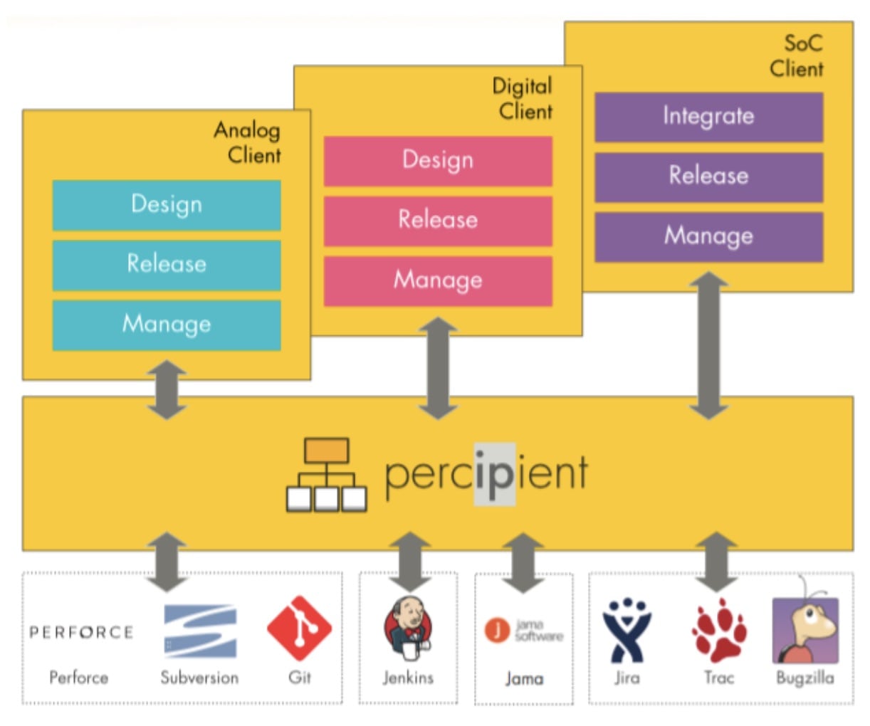
Jerry: Sure, our Percipienttool is an IP Lifecycle Management (IPLM) platform that gives semiconductor design companies control over the design, integration, and traceability of internal IP, external IP, libraries for new analog and digital designs.

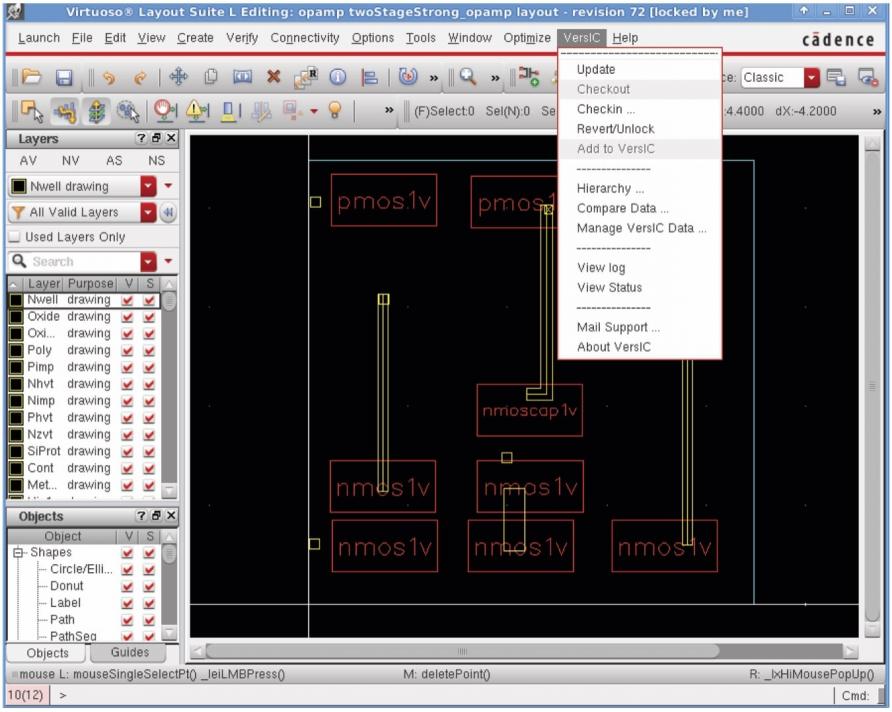
VersIC 2.0 Platform is a new approach to the management of IC design data. It provides a comprehensive, united and reliable design data management (DM) experience in the Cadence design environment.

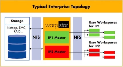
WarpStoraddresses the issue in semiconductor design of data explosion by providing a Content Aware NAS optimizer and accelerator.

Q: Final question, why has Methodics been so successful in the IPLM arena?
Simon: From the beginning, our growth has been driven by our guiding principle to help our customers achieve success in their goals, and this past year was no exception. In addition to maintaining strong relationships with existing customers, we look forward to working with many new customers in 2019 and beyond.
Related Blogs
- SoC Design Partitioning to Save Time and Avoid Mistakes
- Using IP in a SoC Compliant with ISO 26262
- IP Management Using both Git and Methodics


Comments
There are no comments yet.
You must register or log in to view/post comments.