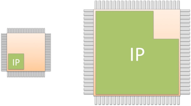
It’s common to see an SoC with a few hundred IP blocks today, which is quite a change from full-custom IC designs developed in the early days (i.e. 1980’s) where there was little IP re-use at all. This shift in the technology and business of IP has created a relatively new industry of IP providers from small to large in size.

Comparison of old vs new SoC (#IP blocks, % of chip that is IP)
There are many new questions about how to bring all of these 3rd party IP blocks together.
- How do you integrate hundreds of IP blocks correctly?
- Are my IP blocks designed correctly?
- Should I re-use hard or soft IP?
- Are my required IP blocks available at 20nm and smaller nodes?
- If the Process Development Kit (PDK) changes, how does that affect my IP blocks?
Early IP Management
One tool that has been used for decades to manage the SoC design process is simply the Excel spreadsheet, it’s ubiquitous, can be programmed to track just about anything, and engineers know how to use it. I could have columns in Excel for IP block name, area, power, company, status, version number, etc.

Using Excel to Manage IP Blocks
If your chip had a handful of IP blocks, then Excel is certainly an adequate tool. If you only have one person tracking IP then Excel works OK, however if you want to share this info with a team or across geographies than Excel sent by email tends to get out of date and is not very efficient.
In the 180nm node era your IP blocks were stable and didn’t have many revisions during your design, however at the newer nodes like 20nm we are getting very early access to IP blocks which will have multiple revisions as the process is being developed in parallel with your design. So with hundreds of IP blocks on a modern SoC, each one at a different stage of completeness, we cannot keep this critical info in our heads or tracked in a simple Excel spreadsheet and expect our chip to work in first silicon. Just one IP block that is out of date, or out of spec will certainly cause a re-spin of silicon, which could be a multi-million dollar added expense.
The Need for IP Management
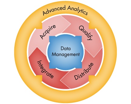
IP has moved beyond simple gates and flip-flops into complete sub-systems like USB, PCI-E and video controllers. Each IP block has a lifecycle that should be understood and tracked. When the IP vendor delivers an updated version of a block, then we must deliver that new version to all our groups worldwide in a controlled manner.
If a new version of IP block effects another IP block (PHY + controller), then the design team needs to be alerted of this connection so that they can re-validate the two blocks together. If you find a bug in your IP, then it needs to be noted, reported, and other designers alerted.
In addition to tracking the status of all IP blocks, a design team needs to know what IP blocks are available so that they can decide to build, re-use or buy a new IP block. Designers should know if they are working on the approved version of IP, and are using the required views – not all possible views.
Design teams spread out across timezones should be able to reproduce the same design environment, quickly and easily, without having to refer to notes or email messages. As IP blocks can contain gigabytes of data, it is most efficient to point to the version you need from a centralized location, instead of making remote copies of it.
Managers on the design team should be able to analyze the tracking of IP, data associated with it, and use of it. This info can help them manage the design process and even compare this SoC project with others.
IP Management Tools
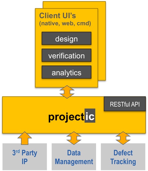
The good news is that engineers from Methodicshave understood the changing IP landscape and created an EDA tool called ProjectIC to help manage each of the issues listed above.
- projectIC from Methodics
- Delivers all of the above and more
- Built on industry standard data management platforms and allows Semiconductor data to live in the same environment as the rest of the project data (firmware, etc).
- Supports analog and digital deisgn and verification methodologies

ProjectIC from Methodics
This tool is built upon industry standard data management platforms (Perforce, Subversion, ClearCase, DesignSync) which allows your semiconductor data to share the same environment as other groups, like firmware, etc. Another benefit of using ProjectIC is that it supports both analog and digital design and verification methodologies.
To learn more about what ProjectIC offers your SoC development team, check out these resources:
Share this post via:


Comments
There are no comments yet.
You must register or log in to view/post comments.