Transistor-level design for full-custom and analog circuits has long been a way for IC design companies to get the absolute best performance out of silicon and keep ahead of the competition. One challenge to circuit designers is meeting all of the specs across all Process, Voltage and Temperature (PVT) corners, so that silicon yields high enough to maximize profits. In the early days of my IC design career at Intel in the 1970’s we had a simple design methodology:
1. Manually size the circuits
2. Run SPICE at TT, FF, SS, SF, FS corners
3. Measure SPICE results, iterate back to step 1 as needed to meet specs
4. Fabricate silicon
5. Measure silicon results, iterate back to step 1 as needed to meet specs
Even today this transistor-level IC design methodology hasn’t changed all that much, except that at step 2 we have circuit designers running Monte-Carlo SPICE either in brute-force or smart methodologies. Step 1 has seen many attempts at automatically sizing transistors. Having to iterate from step 5 all the way back to step 1 means that first silicon didn’t meet specs, so most design teams want to avoid that possibility by all means possible because of the added time and expense of mask sets and fabrication.
Let’s talk about an approach from a new EDA company Intento Designthat directly addresses steps 1-3 in a novel way using a tool called ID-Xplore. I had a recent e-mail dialog with engineers at Intento to learn about their methodology for analog design.
Q: What is so unique about ID-Xplore?
The ID-Xplore Intention view is used to capture the designer’s intentions. Each designer has his own approach to design and the Intention view expresses this in terms of electrical parameters for a given topology. Both the electrical parameters and the circuit schematic are used to control transistor sizing operations during design exploration.
Q: Why optimize electrical parameters?
Design exploration with electrical parameters, rather than transistor size, saves time and provides increased design insight. Electrical parameters describe the controllable, causal relationships between the technology PDK, transistor size and circuit performance. Using electrical parameters allows the designer to ’scrape the bottom’ of the technology kit, looking for extended performance gains and increased control of performance trade-offs.
Because transistor sizing is based on the electrical parameters, ID-Xplore does not need a preliminary sized schematic to start exploration. In addition, electrical parameter exploration is what enables easy technology migration, a core feature of ID-Xplore.
Q: Why is PVT analysis so difficult?
This is an area where analog designers have lost control – literally. Increased technology complexity has meant that intuitively added “design margin” to just doesn’t work anymore. Instead, increased process complexity has led to tool complexity and “design by verification” (basically, a PVT analysis is run, specifications are debugged, and sizing is adjusted to meet performance targets, and so on…).
The result of all this is that designers make many iterations, costing lot of time just to reach a well centered design with enough margin to cover performance over PVT variation.
Q: What are the benefits of using the new ID-Xplore approach?
With advanced integration to the technology PDK and SPICE-accurate sizing provided by ID-Xplore, good circuit design for PVT is at designer’s hands. In other words, design margining is back with Intento approach.
Not only is design margining back – but ‘intuitive’ just met advanced data processing with explicit control and exploration of transistor electrical parameters, rather than size. Now, the designer not only adds margin but really finds exactly where in the design space the PVT analysis should start.
Q: Can you show me how a circuit designer would start to use ID-Xplore?
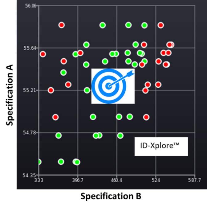
Here is a chart showing circuit performance specifications A and B. Each circle shows the results of SPICE simulation of testbench performance analysis on a fully sized schematic. The testbench performance either meets all specifications (green) or fails to meet one or more specifications (red).
By understanding their specification targets, their topology and the sensitivity of the specifications – the designer can select from within the green cluster of fully satisfying schematic results a sized schematic with enough margin likely to pass PVT.

Simultaneous display of multiple sizing solutions shows the spread of typical performance. Of course, it is a little more complicated because each performance specifications must be compared to all other specifications (the ID-Xplore N-Viewer enables this multidimensional view).
The first step is to create a design space by specifying the range of electrical parameter values. The next steps are:
- • Explore the design using ID-Xplore global exploration
- • Inspect the display of specifications, evaluating critical trade-offs
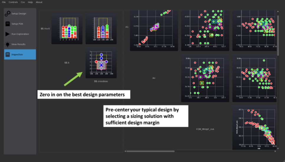
- • Pre-center by selecting the best positioned solution to begin PVT
Here is a picture of the N-Viewer displaying with a handful of well-centered typical results selected:

The electrical parameters describe bias information (transconductance, device current, device length, …) as well as design plan parameters, such as inter-stage current ratios. The N-Viewer cross-probe and cross-select capabilities between the performance specification display and electrical parameter data helps designers to understand the design physics between the circuit topology and the technology PDK models. This improves interpretation on the impact of linear and multi-variate changes where it matters most – in the circuit performance.
Once a well-centered solution is selected, the full circuit transistor size data can be automatically back-annotated to the Open Access database. Next, verify the design by running PVT analysis. A pre-centered design from ID-Xplore typically either passes PVT completely or fails on only a few worst-case corners.
Q: What happens if the schematic with ID-Xplore sizing fails in some corners?
If the first sizing solution fails on some specifications, the designer has several options:
1. Return to the typical results already displayed with a better understanding of the circuit limits, and select a sizing solution with different trade-offs; or,
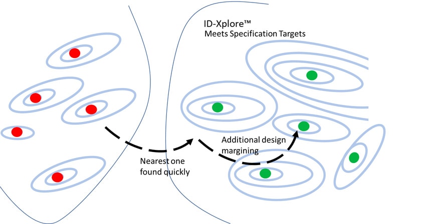
2. Use ID-Xplore directly on PVT corner testbenches. In this situation, ID-Xplore searches the design space for valid solutions as shown below.

Of course, ID-Xplore is all about design insight, and it is also possible to adjust the electrical parameter range, targeting an entirely different performance range based on changing design insight after PVT analysis.
Q: How long does it take for ID-Xplore to execute a typical run?
A design space exploration can take a few minutes, or few tenth of minutes depending on the time for testbench simulation and the number of points in the design space. It is an exploration tool – and finding either accurate trade-off information or good design results quickly of course frees up time to change the schematic and get added performance with additional sub-circuits.
In analog circuit design, transistor sizing is the final target.
With SPICE accurate transistor sizing, full integration with the technology PDK and electrical parameter exploration – transistor size data becomes an output rather than the input of design. From here, designers have full control of which typical sized schematic is best centered for their critical specifications and used in PVT verification.
Related Blogs
- A New Kind of Analog EDA Company
- The Intention View: Disruptive Innovation for Analog Design
- CEO Interview: Ramy Iskander of Intento Design


Comments
4 Replies to “Analog IC design across PVT conditions, something new”
You must register or log in to view/post comments.