


What is Skipper? Well, it seems it’s a penguin in the movie Madagascar. And one of Barbie’s sisters. Who knew? But for Semiwiki readers it’s an integrated chip finishing platform from ICScape. Skipper can read in full-chip layout extremely fast, examine it and manipulate it in various ways, and write it out again.
Skipper solves a number of different problems, both before tapeout and when debugging silicon exhibiting problems:
- True chip finishing, taking the output from the primary design system and producing the file for sending to the mask shop for fabrication
- Debugging a chip when it fails test in a non-obvious way or when a chip fails and the cause needs to be determined
- Interfacing to focused ion beam (FIB) systems for microsurgery and deeper analysis of the chip using the real silicon
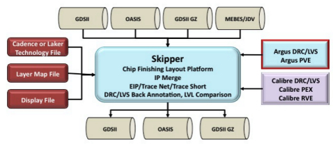
Much of the challenge in handling designs at this stage is their sheer size. For Skipper to have good interactive response then it needs to have the most efficient data structures. After all, even a moderate-sized chip has billions of polygons these days, and if the design is being handled after reticle enhancement (RET) and addition of artifacts like dummy metal fill then the polygon count explodes. Skipper has been optimized for handling designs at the full-chip level in order that it can read, manipulate and write back huge GDS files.In its chip finishing mode, Skipper can:- handle very large layouts (100GB+ files in GDS, Oasis, MEBES etc) with fast load and refresh
- merge in standard cells and IP blocks to replace footprints, switch cells, add seal rings
- make detailed layout changes down to the polygon level
- debug DRC and LVS errors at the full-chip level including setting waivers, eliminating duplicate errors and generating DRC reports
- compare layout between any two full-chip representations including checking individual layers of mask representation versus the original layout (e.g. MEBES vs GDS). This is done using multi-core operating for highest performance

For debugging chips and analyzing failures, Skipper has a number of additional features:- despite not requiring a full technology file or a PDK, it can still trace nets, even the largest nets such as power, ground and clock nets
- failure analysis engineers can pump simulated current into pins of a failed chip to narrow down where a fault may be occurring so as to assist in locating faults to a given area, small enough to be examined in details with scanning electron microscope (SEM)
- cut out an area of the chip across the whole hierarchy for detailed examination
- FIB allows chips to be altered using nano-machining with beams of Gallium ions. Some FIB machines also allow the design to be inspected without requiring a separate SEM pass. One problem is communicating what cuts to make since the FIB machines do not operate directly from mask data. Skipper can create layout/edit directives for use on the FIB machine to ensure accuracy and reduce turn-round times.Skipper is the highest performance chip-finishing environment available today. It is regularly used today on some of the most demanding designs such as large memories at leading memory manufacturers, or large SoCs at leading communications companies.
ICScape’s website page on Skipper is here.


Flynn Was Right: How a 2003 Warning Foretold Today’s Architectural Pivot