The goal for automatic test pattern generation (ATPG) is to achieve maximum coverage with the fewest test patterns. This conflicts with the goals of managing power because during test, the IC is often operated beyond its normal functional modes to get the highest quality test results. When switching activity exceeds a device’s power capability during test, it can have detrimental effects on the IC, such as collapse of the power supply, switching noise, and excessive current that could lead to joule heating and connection failure. These effects lead to false failures, and can damage IC in ways that decrease it’s lifetime.

When planning for power-aware test and creating production test patterns, several techniques should be used to manage power during test. Using the techniques I outline here, scan shift switching—the largest contributor to power usage during test—can typically be reduced from 50% (normal level as even distribution on 1s and 0s) to 25% with minimal impact on test time.
Reduce the clock frequency to allow power to dissipate and reduce the heating and average power. However, this could exacerbate a problem with instantaneous power because the circuit will settle more between the lower frequency clock pulses.
Skew the clocks such that they rise at different points within the cycle, thus reducing instantaneous power. This technique is highly dependent on the clock design, does not help with average power, is circuit dependent and, in some cases will not address localized problems.
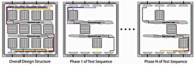
Use a modular test approachto manage switching activity during production test by sequencing test activity and controlling power on a block-by-block basis. This method requires configuring test pattern generation so that only active blocks are considered during the ATPG process and the remaining blocks are held in a steady state.
Manage switching activity during scan test with various ATPG strategies. In standard ATPG, pattern generation targets the maximum number of faults in the minimum number of patterns. This approach leads to high levels of switching activity, usually in the early part of the test set. But if you relax the rate of fault detection and set a switching threshold as part of the initial constraints for ATPG, the coverage rate is spread throughout the entire test set, leading to a lower average switch activity.
Use clock-gating to limit capture power by holding state elements that are not being used to control or observe targeted faults. ATPG controls the clock-gating logic with either scan elements or primary pins. Hierarchical clock controls can provide a finer level of control granularity while using fewer control bits.
Achievable Results
Scan shift switching can typically be cut in half with minimal impact on test time. Capture switching activity can also be significantly reduced, but is highly design dependent. By leveraging features already in place at the system level to control power dissipation in functional mode, power used during production test can be effectively managed. When design-level approaches to power control are combined with ATPG and BIST techniques, you can achieve high-quality test and manage power integrity.For more information on low power testing, download my new white paper “Using Tessent Low Power Test to Manage Switching Activity.”By Giri Podichetty on behalf of Mentor Graphics.


Comments
0 Replies to “Managing Test Power for ICs”
You must register or log in to view/post comments.