The EDA tool offerings for printed circuit board design commonly address one of three customer markets: (1) the enterprise design team, (2) the product development engineer, and (3) the “maker”.
The enterprise pursues complex multi-board systems, often with PCB design teams spanning large organizations – and, typically, with a specialized department of signal integrity, power integrity, EMI, and thermal analysis expertise to support the entire organization. Their tool environment needs to include robust project and configuration management support, enabling a concurrent, collaborative system design of boards, mezzanine cards, and backplane. Complex connectivity model generation is applied for physical verification and electrical analysis.
At the other end of the spectrum, the maker/hobbyist is typically working on simpler designs, as an individual or member of a small design team. The key criterion is this cost of basic PCB design software – often, individuals will utilize low-cost tools (or freeware) for schematic capture and layout. The size and number of board layers is typically limited. Software support usually relies upon on-line help and/or a user group discussion.
A large PCB design market lies between these extremes of the enterprise and the individual. A product development engineering team (or individual engineer) works on a single board, often targeting an unusual product form factor, necessitating aggressive, irregular layouts of power distribution networks (PDN). The development engineers are experts in board physical design and manufacture, but are likely not tool experts.
The complexity of these boards is increasing, as are the performance requirements, due to the integration of more advanced (serial and parallel) interfaces between modules. Signal integrity and power integrity verification can no longer be adequately covered by relatively simple physical design guidelines and electrical rule checks.
These two factors – a small design team facing more difficult projects – necessitate the use of a PCB tool suite that provides:
- an integrated environment: easy to install/maintain, short learning curve
- cost-effective licensing
and especially,
- a rich set of analysis functionality: SI, PI, thermal analysis, EMI validation
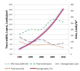
I recently had the opportunity to chat with Paul Musto, Marketing Director, and Jim Martens, Product Marketing Manager for the Board Systems Division at Mentor Graphics, about these PCB design and analysis trends. They provided an interesting graphic depicting how PCB board complexity has increased – please see the figure below. The characteristic measures used are: minimum trace width, number of board layers, and average leads/part (left axis), and the total area and average leads per sq. mm (right axis).
For the enterprise, Mentor offers the Xpedition, HyperLynx, and FloTHERM products. For the development engineering team, PADS is the appropriate tool.
To address the growing analysis requirements for the product development market, Paul and Jim emphasized that Mentor is focused on the evolution of the PADS Product Creation Platform, integrating functionality from the enterprise tools. The new analysis features integrated into the PADS platform functionality is illustrated in the figure below:
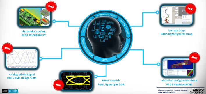
Specifically, Mentor has recently announced the following extensions to the PADS PCB tool suite (at a very affordable cost):
HyperLynx DRC
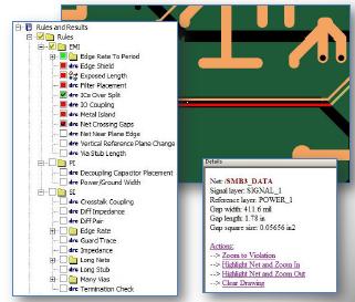
A broad subset of electrical rule checks integrated in HyperLynx DRC is now directly available to PADS users. These rules quickly identify topologies that will likely lead to subsequent issues in EMI and signal integrity analysis – e.g., traces crossing discontinuities such as voids. An example of a HyperLynx DRC report is appended below, illustrating the cross-probing to the PADS physical design.
HyperLynx DC Drop
I*R analysis of the PDN — here’s a link to an earlier semiwiki article highlighting features of the HyperLynx DC analysis now available to PADS users.
PADS FloTHERM XT
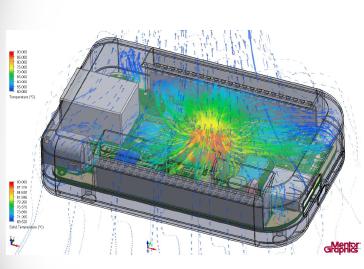
Thermal analysis of the board, embedded in the product enclosure – please see the figure below for an example of the FloTHERM XT analysis.
This new feature expands upon the thermal analysis capabilities currently in the standard PADS offering, with computational fluid dynamics algorithms applied to the 3D model of the board and mechanical enclosure.
Analog simulation (with AMS support)
Users need to exercise board-level simulation incorporating a diverse set of models – e.g., Spice, IBIS, and AMS models from current hardware description languages (which are effective for sensors and electromechanical components).
HyperLynx DDR Wizards
This PCB design market segment has a crucial need to analyze the intricate timing margins and electrical interface requirements of JEDEC DDR/DDR2/DDR3 memory standards. Mentor’s robust DDR “wizards” guide users through the full DDR configuration definition and timing/SI analysis flow, as depicted below.
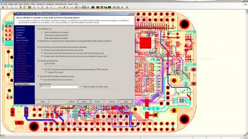
(For more information on Mentor’s DDR Wizard technology, here is a link to an earlier semiwiki article.)
Mentor is offering these additional enterprise-level features in the PADS Product Creation Platform at very attractive license costs – e.g., $3.5K to $5K for a seat of the HyperLynx features.
(Note: PADS FloTHERM XT licensing is higher. Also, there are relatively minor limitations associated with the transfer of these HyperLynx and FlowTherm tools to PADS – e.g., single board designs only, no DDR4 wizard support).
To accelerate training and simplify support, Mentor also offers lots of on-line videos for these tools — a partial list is appended at the end of this article.
There is clearly a market need to support the PCB designer with a comprehensive set of analysis functionality required for today’s products, which incorporate advanced signal interfaces and with stringent thermal form factor and power distribution requirements. Mentor has addressed this need by expanding their mainstream PCB design tool into the PADS Product Creation Platform, at a very affordable cost.
For more information on the PADS Platform, please follow these links to Mentor’s on-line videos.
PADS Product Creation Platform Overview
-chipguy
Share this post via:


Comments
There are no comments yet.
You must register or log in to view/post comments.