![SILVACO 051525 Webinar 400x400 v2[62]](https://semiwiki.com/wp-content/uploads/2025/04/SILVACO_051525_Webinar_400x400_v262.jpg)


In Silvaco’s July 2025 video presentation at the 62nd Design Automation Conference (DAC), Senior Staff Applications Engineer Tim Colton introduced Jivaro, a specialized parasitic reduction tool designed to tackle the escalating challenges of post-layout simulation in advanced IC designs. As semiconductor nodes shrink and designs grow more intricate—mirroring the AI chip complexity outlined in Synopsys’ guide parasitics explode, inflating simulation runtimes. Jivaro, in production for over 15 years, stands out as a standalone solution that accelerates simulations by 2x to 15x without sacrificing accuracy, fitting seamlessly between extraction and simulation stages.
Colton emphasized the tool’s core value: enhancing designer productivity amid tightening cycles. For instance, a simulation dropping from seven days to three enables multiple iterations daily, fostering innovation. This aligns with Synopsys’ “shift-left” methodology, where early optimization reduces risks. Jivaro’s process- and node-agnostic nature—operating on DSPF databases—ensures broad applicability, from FinFET nodes to high-speed analog blocks. It strips dummy devices in lower nodes, streamlining simulator workloads.
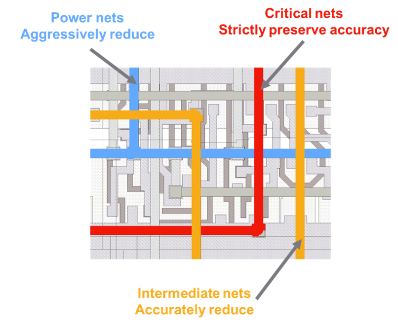
Key features include customizable reduction. Users categorize nets—power (aggressive reduction), intermediate (balanced), and critical (high accuracy)—tailoring accuracy to 1% on sensitive paths while aggressively pruning others. Multi-finger device merging connects parallel transistors textually, slashing device counts by up to 30% and runtime accordingly. In one example, a 10k-transistor 5nm analog block saw simulation time halve from five hours using embedded extractor reduction, then quartered to 1.25 hours with Jivaro’s selective settings. For larger designs, a 20-day run compressed to 10 days, enabling previously infeasible analyses.
Advanced capabilities like guarded parasitic reduction preserve signal integrity in high-accuracy scenarios. A recent enhancement, driven by customer feedback from a major cellphone producer, replaces MOS caps (three-pin transistors) with two-pin capacitors, yielding an additional 2x speedup on RF designs already optimized 3x. This underscores Jivaro’s evolution, supporting markets like displays, power devices, and AI-driven SoCs.
Real-world adoption validates its impact. Customers like Silicon Creations (PLLs), Etopus (PHYs), and Alpine leverage Jivaro for iterative, high-precision workflows. By offloading simulations to smaller machines, it optimizes resource use, addressing talent and cost constraints in the $383B AI chip market by 2032.
Ultimately, Jivaro exemplifies how targeted EDA tools master complexity. As AI workloads demand scalable silicon, solutions like this—echoing Synopsys’ holistic approach—ensure first-pass success, boosting coverage without accuracy trade-offs. Colton’s demo positions Silvaco as a vital ecosystem player, accelerating the journey from big ideas to breakthroughs.
About Silvaco Group, Inc.
Silvaco is a provider of TCAD, EDA software, and SIP solutions that enable semiconductor design and digital twin modeling through AI software and innovation. Silvaco’s solutions are used for semiconductor and photonics processes, devices, and systems development across display, power devices, automotive, memory, high performance compute, foundries, photonics, internet of things, and 5G/6G mobile markets for complex SoC design. Silvaco is headquartered in Santa Clara, California, and has a global presence with offices located in North America, Europe, Egypt, Brazil, China, Japan, Korea, Singapore, Vietnam, and Taiwan. Learn more at silvaco.com.
Also Read:
Silvaco’s Diffusion of Innovation: Ecosystem Investments Driving Semiconductor Advancements
Analysis and Exploration of Parasitic Effects
Silvaco: Navigating Growth and Transitions in Semiconductor Design
Share this post via:


Comments
There are no comments yet.
You must register or log in to view/post comments.