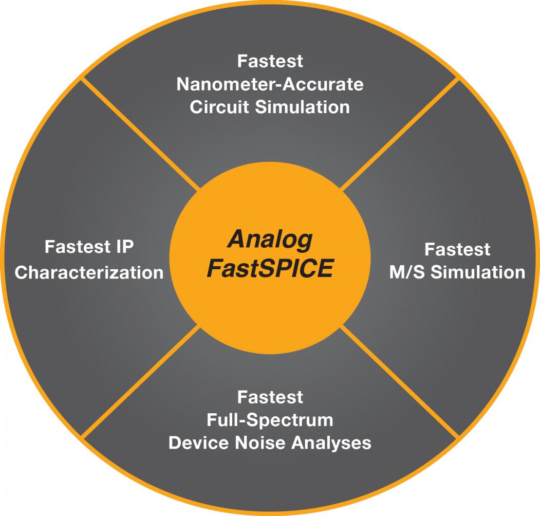
 Analog, mixed-signal, RF, and custom digital circuitry implemented in GHz nanometer CMOS introduce a new class of design and verification challenges that traditional transistor‑level simulators cannot adequately address. Berkeley Design Automation, Inc., (BDA) was founded in 2003 by Amit Mehrotra and Amit Narayan, UC Berkeley Ph.D. graduates within the intent of delivering a next-generation circuit-level design tools to address these coming challenges. Ravi Subramanian, another UC Berkeley Ph.D., joined shortly thereafter as CEO. Together, and with initial funding from Woodside Fund and Bessemer Venture Partners, the three embarked on launching the venture.
BDA’s initial focus was to deliver full-spectrum device noise analysis for high-performance analog and RF ICs based on Mehrotra’s fundamental research contributions. In 2004, the company introduced its initial product, PLL Noise Analyzer™, the first tool in the industry to provide closed-loop transistor-level device noise analysis tool phase-locked loops (PLLs). Through establishing the tool in several leading-edge semiconductor companies, BDA positioned itself to learn about design teams’ most significant circuit design and verification challenges—all of which required breakthrough accuracy, performance, and capacity. BDA was able to leverage the different technologies it developed for the PLL Noise Analyzer to create a new nanometer circuit verification platform that would deliver just that.
In 2006, BDA introduced the centerpiece of its new platform—the Analog FastSPICE™ circuit simulator (AFS). The product’s simple yet powerful value proposition was anchored on delivering identical results to traditional SPICE with 5×–10× higher performance and 5x-10x higher capacity that was plug-compatible with existing flows. With this breakthrough capability, design teams could solve analog/RF circuit verification problems that were previously impossible or infeasible using traditional SPICE. Thus, the new simulator category “Analog FastSPICE” was born—“Analog” accuracy with ”fastSPICE” performance.
In order to establish itself in a market crowded with legacy tools, BDA developed its now well-known engagement model of solving problems that design teams literally could not address with their current tools. Generally this consisted of simulating circuits at one or two levels of hierarchy above what they could currently simulate, running circuit simulations in days that would otherwise take weeks, and simulation circuits that otherwise ran in digital fastSPICE simulators – all with foundry certified SPICE accuracy and a drop-in use model. Word spread that SPICE wasn’t dead.
Design teams rapidly adopted AFS and encouraged BDA to deliver even more performance and capacity without compromising accuracy. They also asked BDA to extend AFS functionality to address new nanometer CMOS verification needs, including device noise impact on all noise-sensitive circuits, large post-layout simulations, complex mixed-signal simulation, and efficient characterization of global and local process variation. Leveraging its modular architecture implemented as a unified executable, BDA rapidly filled out the AFS Platform, including: multithreaded and multi-core parallel execution, >10-M element DC and transient capacity, >100K-element periodic steady state analysis, full-spectrum periodic noise analyses, full-spectrum transient noise analysis, and HDL co-simulation. All of these capabilities provide foundry certified accuracy to 20nm for both leading netlist and model formats.
The company’s technology development pipeline continues unabated with leading-edge development to breakdown remaining and emerging barriers. Most recently BDA announced breakthrough AMS capabilities in its Analog FastSPICE AMS simulator which uniquely works with any leading HDL simulator and makes mixed-signal simulation practical for everyday use.
Today, over 125 semiconductor companies around the world rely on the BDA AFS Platform and the company’s deep application expertise to meet their nanometer circuit design and verification challenges. The main circuit application areas include: high-speed I/O, PLLs/DLLs, ADCs/DACs, image sensors, transceivers, memories, and RFICs.
BDA was recognized as one of the 500 fastest growing technology companies by revenue in North America in both 2011 and 2012 by Deloitte. The company is privately held and backed by Woodside Fund, Bessemer Venture Partners, Panasonic Corp., NTT Corp., IT-Farm, and MUFJ Capital.
Share this post via:


Musk’s Orbital Compute Vision: TERAFAB and the End of the Terrestrial Data Center