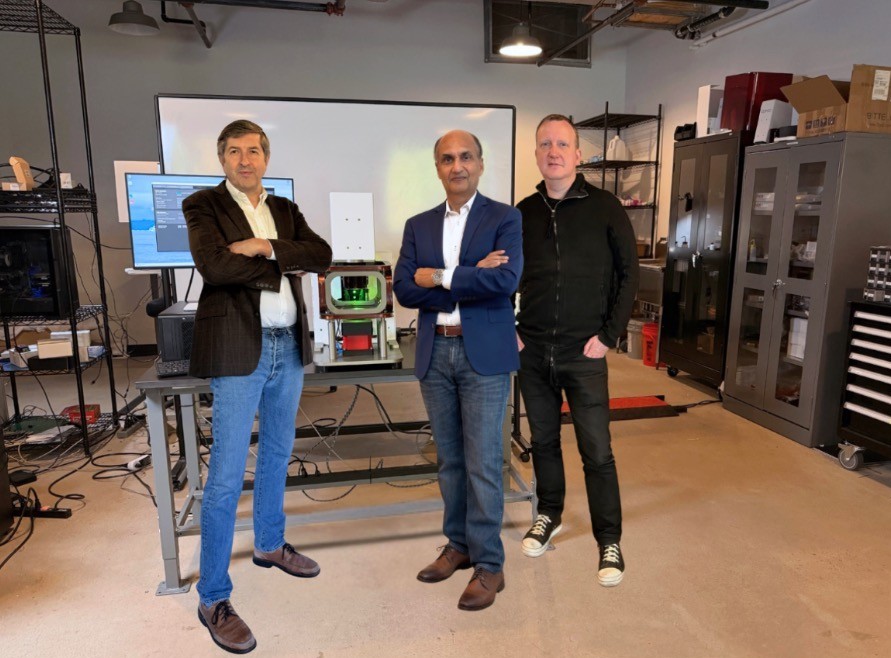
Sanjive Agarwala is co-founder and CEO of EuQlid, a quantum technology company, developing novel 3D imaging tools to support the design and manufacturing of semiconductors and batteries.
Prior to EuQlid, Sanjive served as Corporate Vice President and General Manager of the IP Group at Cadence Design Systems. His business included silicon proven analog, advanced memory interfaces, high-speed SerDes IPs that are all based on industry-standard protocols and Tensilica Processor IP system solutions, with a focus on expanding the Cadence IP portfolio and enabling customers to get their system-on-chip (SoC) products to market faster and with higher quality.
Prior to Cadence, Sanjive was at Texas Instruments, where he led the development of the company’s digital signal processing, artificial intelligence, and digital/analog platform technology, as well as high-end SoCs targeting automotive, industrial, and wireless base-station applications.
Tell us about your company?
EuQlid, a quantum technology company, is developing novel 3D imaging tools to support the design and manufacturing of semiconductors and batteries. Our technology addresses a critical gap in the semiconductor and energy storage industries, visualizing sub-surface currents with precision and speed, where today’s inspection and test tools cannot reach.
What problems are you solving?
The insatiable compute demand of AI is driving semiconductor logic, memory and advanced packaging technologies to adopt complex 3D architectures. New metrology and inspection tools are needed to control and optimize increasingly complex manufacturing workflows. Global demand for advanced metrology and inspection tools exceeds $10 billion annually and is growing rapidly with the adoption of 3D architectures.
Metrology plays a crucial role in semiconductor manufacturing by providing detailed information on the physical properties of silicon and packages. Process engineers make control adjustments to meet specific product parameters, ensuring the production of reliable semiconductor devices of high quality while minimizing waste. Effective metrology is therefore essential for maintaining the economic viability and sustainability of the overall manufacturing process.
EuQlid’s proprietary quantum 3D imaging platform, Qu-MRITM, enables non-destructive mapping of buried current flow with precision and speed that are unmatched in the industry.
What application areas are your strongest?
The next era of semiconductor scaling will be driven by 3D heterogeneous integration (3DHI) and novel 3D logic and memory architectures. EuQlid’s 3D imaging platform meets or surpasses precision and speed requirements to enable measurement of sub-surface currents and thereby determine the integrity of buried and invisible device structures. The semiconductor industry today is valued at over $600B annually and heading to $1T+ by 2030. Inspection and metrology tools have always been an integral part of manufacturing, and demand continues to grow with the increasing complexity of manufacturing workflows.
Similarly, with the “electrification of everything” revolution, energy storage devices are undergoing significant innovation and growth, and will continue to do so for decades to come. Improving battery lifetime, safety and performance requires understanding exactly how and where degradation initiates and propagates. EuQlid’s magnetic imaging platform enables visualization of the spatial and temporal current heterogeneities key to battery health monitoring and charge estimation.
What keeps your customers up at night?
Semiconductor industry leaders like TSMC, Intel and Samsung spend tens of billions of dollars annually in advancing core semiconductor technology and building manufacturing facilities. World economies are dependent on their ability to manufacture and ship flawless semiconductor products. The complexity of these devices and manufacturing flows puts immense pressure on them to stay ahead of the game with best-in-class design and manufacturing tools. They rely on companies like EuQlid to innovate and provide the metrology tools needed to deliver their products.
What does the competitive landscape look like and how do you differentiate?
Metrology is adapting to meet the varied demands and integration techniques required by different 3DHI workflows. Technologies such as X-ray fluorescence (XRF), atomic force microscopy (AFM), ellipsometry, and white-light interferometry provide engineers with unprecedented precision and capabilities, but they also have their limitations. EuQlid is addressing the whitespace in buried interconnect opens, shorts and non-wet defect inspection for in-line metrology applications.
What new features/technology are you working on?
EuQlid is developing the full-stack Qu-MRI platform combining quantum magnetometry with advanced signal processing and machine learning to deliver buried electrical current maps with high-throughput and nano-amp sensitivity without physical contact or destructive cross-sectioning.
The technology platform is being used to analyze customer samples representing their tough problems which require innovative solutions going forward.
How do customers normally engage with your company?
Customers engage with us by reaching out directly through our academic and industry networks. They can also reach us online through our website (euqlid.io) or LinkedIn.
Also Read:
CEO Interview with Wilfred Gomes of Mueon Corporation
CEO Interview with Alex Demkov of La Luce Cristallina
CEO Interview with Dr. Bernie Malouin Founder of JetCool and VP of Flex Liquid Cooling
Share this post via:


Silicon Insurance: Why eFPGA is Cheaper Than a Respin — and Why It Matters in the Intel 18A Era