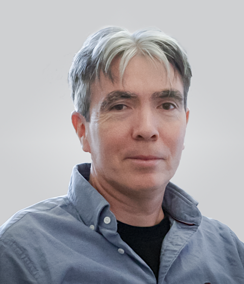
Dr. Josep Montanyà Chief Executive Officer – UK/Spain Co-founder leading the company, with +18 years of experience in MEMS, patents and the semiconductor industry. Founded Baolab Microsystems prior to Nanusens.
Tell us a little bit about your company?
We have a patented technology that allows us to build chips with nano-mechanisms inside (called NEMS) using the de facto standard manufacturing for solid state chips (called CMOS). This allows us to have better performance, smaller size and lower cost.
There are many applications for this technology, including sensors, RF tunable devices and even AI processors with higher speeds and less consumption. Our initial focus is on a particular product called RF DTC (Digitally Tunable Capacitor). We have a very clear route to market, with signed LOI, and we will place it into Tier 1 phones (and more) that will hit the market in 4 years.
Beyond this initial product there are more RF devices we can build, and a large variety of sensors. Until now inside each wearable or portable system, you have a digital processor and one or more external sensors chips. We have the capability to change this, by embedding the sensors into the digital processors. Today it is possible to do this by using complex multi-die packages. We don’t need to do that. Instead, at Nanusens, we can build all these sensors monolithically on the same CMOS die where the digital processor is built. And this is done without impacting yield and using minimal additional area. This reduces dramatically the size of the overall system, and it reduces also power consumption to levels that today are unseen.
The company is split between its HQ in Paignton (UK) and a subsidiary in Cerdanyola (Spain).
What was the most exciting high point of 2024 for your company?
This year we got our RF DTC prototype measured by a large corporation. This was a very important milestone, because not only it shows the interest of the industry in our product, but it also validated all our measurements.
These measurements proved the incredible performance that our RF DTC can achieve, and it has helped us to better understand our route to market. Being able to increase by 30% the antenna efficiency of cell phones means that we increase by 30% talk time, we also increase by 14% the range from the base antenna, meaning that many areas of poor reception disappear. And for the smartphone OEM, the size of the PCB can be reduced, given that with our solution there is no need to switch standalone external capacitors. Reducing PCB size inside the phone is a key driver for smartphone OEMs, as this means having more space for battery.
With our chip, we aim to monopolize the +$800m market of smartphone aperture antenna. This is because we have unmatched performance, small size and low cost. And all this comes from the fact that we use our patented technology to build NEMS devices in CMOS.
What was the biggest challenge your company faced in 2024?
Main difficulty for a pre-revenue start-up like Nanusens developing semiconductor and even more MEMS technology is fundraising. Our goal for 2024 on this front was to raise a £8m Series A to provide prototypes of inertial sensor and RF DTC devices, so that next year we would be in the market with our first products, and we have customers waiting for them. This has been moved to 2025 as we will have achieved more significant milestones by then that will facilitate this process.
How is your company’s work addressing this biggest challenge?
We have decided to focus on the RF products, leaving sensors and other devices in our future roadmap. This has allowed us to reduce costs and be more efficient.
What do you think the biggest growth area for 2025 will be, and why?
I think AI processors will keep being the dominant area in semiconductors. The incredible success of NVIDA, plus all the big techs jumping in, forecasts a very interesting year. At the same time, however, the market is starting to adjust itself, and I believe we will start seeing more start-up failures in this field as well. You need something really different to succeed in such a competitive field, dominated by giant players.
How is your company’s work addressing this growth?
We put a limited effort on studying the possibility to build better AI processors using our NEMS in CMOS technology. We discovered that it is possible for us to build vacuum transistors in CMOS. This has the potential to enable x10 faster AI processors and consuming half of the power.
Vacuum transistors enjoy the terahertz range bandwidths of vacuum tubes, but without their problems of large size, mechanical fragility, low reliability and large power consumption. In fact, given the very small, nano-sized gaps of vacuum tubes, there is not even a need for heating the metals at high temperatures. Instead, a low voltage generates such a strong electrical field with this small gap, that electrons fly between the cathode and the anode by field emission.
There are research papers on vacuum transistors, which have been built using custom NEMS processes. At Nanusens, we have the capability to build them using standard CMOS processing. This has the potential to build AI processors far beyond the state of the art, and with a process ready to produce them in high volumes. This is a project for after the Series A round is completed.
How do customers engage with your company?
Although technically we can sell IP and have already done so, our business model is to sell product (ICs) directly to our customers or through distributors.
Additional questions or final comments?
It is always difficult to predict the future. But 2025 will be a very interesting year. I will be especially interested to see what happens in this race for dominating the AI digital processor market. But, whoever wins this next year, we have a technology that will overpass them in the next years!
Also Read:
CEO Interview: Marc Engel of Agileo Automation
CEO Interview with Dr. Dennis Michaelis of GEMESYS
CEO Interview: Slava Libman of FTD Solutions
Share this post via:


Musk’s Orbital Compute Vision: TERAFAB and the End of the Terrestrial Data Center