You are currently viewing SemiWiki as a guest which gives you limited access to the site. To view blog comments and experience other SemiWiki features you must be a registered member. Registration is fast, simple, and absolutely free so please,
join our community today!
WP_Term Object
(
    [term_id] => 31
    [name] => GlobalFoundries
    [slug] => globalfoundries
    [term_group] => 0
    [term_taxonomy_id] => 31
    [taxonomy] => category
    [description] =>
    [parent] => 158
    [count] => 245
    [filter] => raw
    [cat_ID] => 31
    [category_count] => 245
    [category_description] =>
    [cat_name] => GlobalFoundries
    [category_nicename] => globalfoundries
    [category_parent] => 158
    [is_post] =>
)
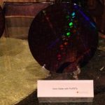
At DAC in Austin a design company, foundry and EDA vendor teamed up to present their experiences with 14nm FinFETs during a breakfast on Tuesday.
Panelists included:
…
Read More
Global Foundries will be at DAC in booth 1314. There will be 6 pods there demonstrating:
- Advanced Technology: 28nm ready and ramping, and next is 20LPM and 14XM.
- PDKs: For 28nm, 20nm and 14nm. 14nm handles FinFET enablement complexity. Robust, easy to use and high quality, supports pretty much the full range of EDA tools.
- Design
…
Read More
EDA needs more CEOs like Amit Gupta. Solido, which is now profitable, is his second AMS EDA company. The first, Analog Design Automation (ADA), was purchased by Synopsys for a hefty multiplier. Prior to becoming an EDA entrepreneur, Amit was product manager for the wireless group at Nortel and a hardware engineer for the RF communications… Read More
I hosted a webinar today for GlobalFoundries. Yes, I know that today was TSMC’s Technology Symposium, we weren’t that smart when we picked the date. It was basically a “fireside chat” with me as the moderator asking the questions and Paul Colestock and Aabid Husain as my guests. We actually did it at Cadence… Read More
The world is analog and despite enormous SoCs in the most leading-edge process node being the most glamorous segment of the semiconductor industry, it turns out that one of the fastest growing segments is actually analog and power chips in older process technologies. Overall, according to Semico, analog and power ICs, including… Read More
In the 1980s, Japan was seen as the leader in the semiconductor industry. Their quality was higher, especially in memories, and the US was worried about falling behind. In fact Sematech was created in 1987 by the US government and a consortium of 14 US-based semiconductor companies primarily to pool investment on common problems… Read More
As you know, I’ve been a bit of a bear about what is happening to wafer costs at 20nm and below. At the Common Platform Technology Forum last week there were a number of people talking about this in presentations and at Harvey Jones’s “fireside chat”.
At the press lunch I asked about this. There are obviously… Read More
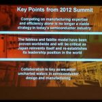
FinFETs are hot, carbon nanotubes are cool, and collaboration is the key to continued semiconductor scaling. These were the main messages at the 2013 Common Platform Technology Forum in Santa Clara.
The collaboration message ran through most presenations, like the afternoon talk by Subi Kengeri of GLOBALFOUNDRIES and Joe Sawicki… Read More
I spent some quality time with Subi Kengeri, Vice President, Technology Architecture, Office of the CTO, GLOBALFOUNDRIES in Las Vegas during CES. Great guy, he worked at Silicon Access, Virage and TSMC before GF. One thing you should know about embedded memory guys, SRAM is the first thing that goes through a new process so they … Read More
GLOBALFOUNDRIES changed the landscape of the foundry business in 2009 with a simple but ambitious plan to become the world’s first truly global foundry. At the Common Platform Technology Forum February 5th in the Santa Clara Convention Center GF Executive Vice President Michael Noonen will give an update on how that is … Read More


Unraveling Dose Reduction in Metal Oxide Resists via Post-Exposure Bake Environment