
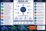
Advanced semiconductor systems are no longer limited by a single engineering domain. They are constrained by the convergence of many interdependent vectors: silicon nodes, advanced packaging architectures, substrate materials, platform PCBs, power-delivery networks, thermal behavior, manufacturing variation, firmware… Read More
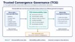
From Evidence to Authority: Bounded Gate Authority for Governed Semiconductor Realization


Intel: Pushing EMIB Forward: Design Methodology Insights with Synopsys Tools