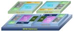
Today Alchip Technologies, a Taipei-based leader in high-performance and AI computing ASICs, announced a significant milestone with the successful tape-out of its 3D IC test chip. This achievement not only validates Alchip’s advanced 3D IC ecosystem but also positions the company as a frontrunner in the rapidly evolving field… Read More
At the recent Hot Chips conference, Intel® unveiled Clearwater Forest, its next-generation Xeon® 6 processor with efficiency cores (E-cores). The unveiling was made by Don Soltis, Xeon Processor Architect and Intel Fellow with over four decades of processor design experience and a long-standing contributor to the Xeon roadmap.… Read More
Dan is joined by Dr. Julien Ryckaert who joined imec as a mixed-signal designer in 2000, specializing in RF transceivers, ultra-low power circuit techniques, and analog-to-digital converters. In 2010, he joined imec’s process technology division in charge of design enablement for 3DIC technology. Since 2013, he oversees… Read More
Todd Burkholder and Andras Vass-Varnai, Siemens EDA
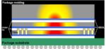
As semiconductor devices become smaller, more powerful and more densely integrated, thermal management has shifted from an afterthought to a central challenge in modern IC design. In contemporary 3D IC architectures—where multiple chiplets are stacked and closely arrayed—power… Read More
PDF Solutions has been around for over 30 years. The company began with a focus on chip manufacturing and yield. Since the beginning, PDF Solutions anticipated many shifts in the semiconductor industry and has expanded its impact with enhanced data analytics and AI. Today, the company’s impact is felt from design to manufacturing,… Read More
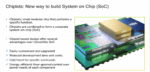
As multi-die and chiplet-based system designs become more prevalent in advanced electronics, much of the focus has been on physical design challenges. However, verification—particularly functional correctness and interoperability of inter-die connections—is just as critical. Interfaces such as UCIe or custom interconnects… Read More
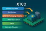
imec XTCO (Cross-Technology Co-Optimization) is the natural successor to DTCO and STCO in an era where no single layer of the stack can deliver scaling alone. Instead of optimizing devices, interconnect, packaging, architecture, and software in isolation, XTCO treats them as one tightly coupled system with a shared budget … Read More
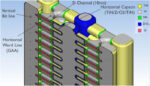
Epitaxial stacks of silicon and silicon germanium are emerging as a key materials platform for three dimensional dynamic random access memory. Future DRAM will likely migrate from vertical channels to horizontally stacked channels that resemble the gate all around concept in logic. That shift demands a starter material made… Read More
As we all know, the age of multi-die design has arrived. And along with it many new design challenges. There is a lot of material discussing the obstacles to achieve more mainstream access to this design architecture, and some good strategies to conquer those obstacles. Synopsys recently published a webinar that took this discussion… Read More


Chemical Origins of Environmental Modifications to MOR Lithographic Chemistry