As semiconductor technology advances into increasingly complex and expensive process nodes, the economic and technical risks associated with ASIC design have grown dramatically. At advanced nodes such as Intel 18A, the cost of a single design error can escalate into tens of millions of dollars, compounded by months of delay.… Read More

Author: Daniel Nenni
Silicon Insurance: Why eFPGA is Cheaper Than a Respin — and Why It Matters in the Intel 18A Era

Chemical Origins of Environmental Modifications to MOR Lithographic Chemistry

In the pursuit of advanced extreme ultraviolet (EUV) lithography for high-NA patterning, metal oxide resists (MORs) offer significant promise but face challenges like critical dimension (CD) variation due to atmospheric interactions. Presented at SPIE Advanced Lithography + Patterning 2025 by Kevin M. Dorney and colleagues… Read More
GTC 2026: Agentic AI for Semiconductor Design and Manufacturing

Beyond Moore’s Law: High NA EUV Lithography Redefines Advanced Chip Manufacturing

The imec installation of the ASML EXE:5200 High Numerical Aperture (High NA) extreme ultraviolet (EUV) lithography system at imec represents a pivotal advancement in semiconductor manufacturing and research. This system, installed in imec’s 300 mm cleanroom in Leuven, Belgium, introduces unprecedented lithographic resolution… Read More
CEO Interview with Moti Margalit of SonicEdge

Moti Margalit is the CEO and co-founder of SonicEdge, a deep-tech pioneer reinventing sound through ultrasonic modulation – unlocking smaller, vibration-free speakers with studio-quality audio.
With a background in lasers and electro-optics, Moti transitioned from technologist to inventor. His career spans 150+ patents… Read More
WEBINAR: Reclaiming Clock Margin at 3nm and Below

At 3nm and below, clock networks have quietly become the dominant limiter of SoC power, performance, and yield. Yet most advanced-node designs still rely on abstraction-based signoff methodologies developed when voltage headroom was generous and interconnect effects were secondary.
That assumption no longer holds
As supply… Read More
Verification Analytics: The New Paradigm with Cogita-PRO at DVCON 2026
Cogita-PRO, developed by Vtool, introduces a transformative approach to design verification by treating it as a big data challenge rather than a traditional debugging exercise. Released in February 2026, this tool shifts the focus from manual log and waveform inspection to advanced verification analytics powered by data … Read More
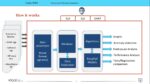
AI-Driven Automation in Semiconductor Design: The Fuse EDA AI Agent

The semiconductor industry is experiencing unprecedented growth in complexity as advanced process nodes, heterogeneous integration, and AI-driven workloads demand increasingly sophisticated chip designs. At the same time, semiconductor companies face rising design costs, increasing engineering workloads, and a shrinking… Read More
TSMC Technology Symposium 2026: Advancing the Future of Semiconductor Innovation

One of my favorite times of the year is coming (sailing season) and my favorite event of the year is coming as the company I most respect will host the best international semiconductor networking event starting here in Silicon Valley.
The 32nd annual TSMC Technology Symposium represents one of the most influential events in the … Read More
Unraveling Dose Reduction in Metal Oxide Resists via Post-Exposure Bake Environment

In the realm of extreme ultraviolet (EUV) lithography, metal oxide resists (MORs) have emerged as promising candidates for advanced semiconductor patterning. However, their stability poses challenges, particularly interactions with clean-room environments like humidity and airborne molecular contaminants (AMCs) … Read More


Musk’s Orbital Compute Vision: TERAFAB and the End of the Terrestrial Data Center