You are currently viewing SemiWiki as a guest which gives you limited access to the site. To view blog comments and experience other SemiWiki features you must be a registered member. Registration is fast, simple, and absolutely free so please,
join our community today!
Posts Search Results for "3dblox"
There was a lot of discussion at IEDM about the coming shift to gate-all-around (GAA) transistor structures. This new device brings many benefits to continue device scaling, both at the monolithic device level as well as for multi-die design. The path to GAA is not simple, there are new material, process and design considerations… Read More
The main program for the 70th IEDM opened on Monday morning in San Francisco with an excellent keynote from Dr. Yuh-Jier Mii, Executive Vice President and Co-Chief Operating Officer at TSMC. Dr. Mii joined TSMC in 1994. Since then, he has contributed to the development and manufacturing of advanced CMOS technologies in both fab
…
Read More
At the recent TSMC OIP Ecosystem Forum in Santa Clara, there was an important presentation that laid the groundwork for a great deal of future innovation. Alchip and its IP and EDA partner Synopsys presented Efficient 3D Chiplet Stacking Using TSMC SoIC. The concept of 3D, chiplet-based design certainly isn’t new. SemiWiki maintains… Read More
At the 2024 TSMC OIP Ecosystem Forum, one of the technical talks by TSMC focused on maximizing 3DIC design productivity and rightfully so. With rapid advancements in semiconductor technology, 3DICs have become the next frontier in improving chip performance, energy efficiency, and density. TSMC’s focus on streamlining the… Read More
The 2024 live conferences have been well attended thus far and there are many more to come. The next big event in Silicon Valley is the TSMC Global OIP Ecosystem Forum on September 25th at the Santa Clara Convention Center. I expect a big crowd filled with both customers and partners.
This is the 16th year of OIP and it has been an honor… Read More
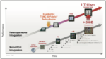
Heterogeneous multi-die integration is gaining more momentum all the time. The limited roadmap offered by Moore’s Law monolithic, single-die integration has opened the door to a new era of more-than-Moore heterogeneous integration. The prospects offered by this new design paradigm are exciting and the entire ecosystem is… Read More
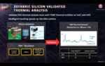
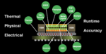
An emerging trend with IC design is the growing use of chiplets and even 3D IC designs, as the disaggregated approach has some economic and performance benefits over a single SoC. There are thermal challenges with using chiplets and 3D IC designs, so that means that thermal analysis has become more important. I just spoke with Michael… Read More
The TSMC Technology Symposium provides a worldwide stage for TSMC to showcase its advanced technology impact and the extensive ecosystem that is part of the company’s vast reach. These events occur around the world and the schedule is winding down. TSMC covers many topics at its Technology Symposium, including industry-leading… Read More
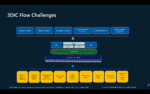
At the recent User2user conference, Amit Kumar, Principal Hardware Engineer, Microsoft, shared the company’s experience from building a 3DIC SoC and highlighted Siemens EDA tools that were used. The following is a synthesis of core aspects of that talk.
3DIC Challenges
Despite the numerous advantages of 3DIC technology, its… Read More
We all know that making advanced semiconductors is a team sport. TSMC can innovate the best processes, but without the right design flows, communication schemes and verified IP it becomes difficult to access those processes. Synopsys recently announced some details on this topic. It covers a lot of ground. The graphic at the top… Read More
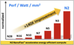


TSMC N3 Process Technology Wiki