

Extreme-ultraviolet lithography is essential for manufacturing advanced semiconductor devices, but its continued scaling presents a difficult materials problem. Photoresists must simultaneously provide high resolution, low exposure dose, limited line-edge or linewidth roughness, and extremely low defectivity. … Read More
Meet Quadric on the Road: Three Must-Attend AI EventsThis late summer, Quadric is taking its vision…Read More
PDF Solutions’ Exensio Was Built for Semiconductor Analytics. The New Exensio Aurora Architecture Is Built for Semiconductor Intelligence.The semiconductor industry doesn't have a shortage of…Read More
Beyond Moore: Co-Optimizing AI from Systems to Materials System Technology Co-optimization in…Read More
Focusing on the AI Big Picture with Moores Lab AI at DAC 2026DAC 2026 proved that agentic AI design flows…Read MoreCEO Interview with Ajit Prabhu of Quest Global
Ajit Prabhu is the Co-Founder and CEO of Quest Global, a global engineering services company driven by a single purpose: to be the most trusted partner for solving the world’s hardest engineering problems. Under his leadership, Quest Global has built long-term, sustainable partnerships and delivers end-to-end engineering… Read More
The Twelve-Month Rule Does Not Describe a New Fab
By Nikhil Shah
Capital spending is often treated as if it becomes semiconductor capacity about twelve months later. That can be a useful rule for equipment installed in an existing fab. It is a poor description of a new fab built from the ground up.
I tested the distinction using five advanced-node projects in the United States where… Read More
CEO Interview with Sumeet Kumar of Innatera
Dr. Sumeet Kumar is CEO of Innatera, the pioneering Dutch neuromorphic processor company. Dr. Kumar was previously with Intel and Indrion Technologies, and has spent his career in microprocessor development. He co-founded Innatera in 2018 as a spin off from the Delft University of Technology.
Tell us about your company?
When… Read More
Podcast EP362: An atomic layer in compute. A discussion of what can be built as graphene photonics scales with Cedric Huyghebaert
Daniel is joined by Dr. Cedric Huyghebaert, CTO of Black Semiconductor. Cedric is one of the world’s leading experts in the development and integration of 2D materials, particularly graphene, into industrial semiconductor manufacturing. With a PhD in Physics from KU Leuven and over 25 years at imec, Cedric built and led… Read More
How TSMC Is Wiring the AI Era With Light
TSMC’s photonics strategy is centered on integrating optical input-output with advanced logic, rather than selling conventional optical transceivers as standalone products. The company is developing a silicon-photonics foundry platform and a packaging architecture called TSMC-COUPE, or Compact Universal Photonic … Read More
Intel Eyes a Memory Comeback as AI Rewrites Chip Economics
Intel is considering a return to memory technology decades after abandoning mainstream DRAM and, more recently, selling its NAND business. Chief executive Lip-Bu Tan has argued that memory should no longer be viewed simply as a low-margin commodity. Artificial intelligence is turning bandwidth, latency and data movement … Read More
Agentrys Shows You How to Build a Multi-Agent System in 30 Minutes
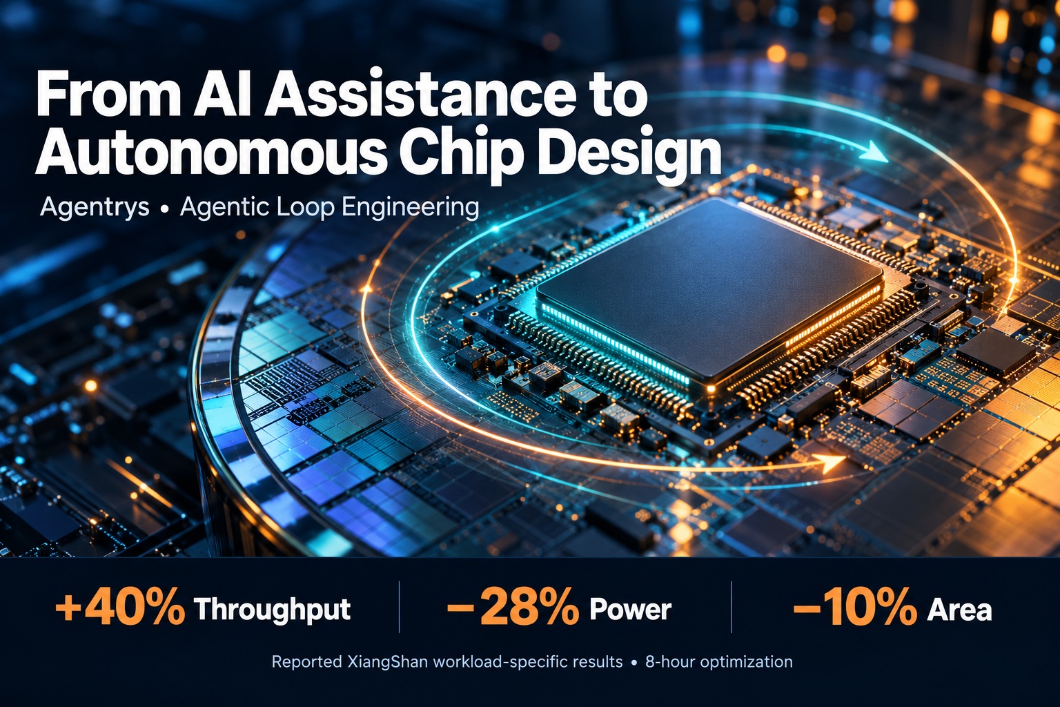
Agentrys believes that a purpose-built multi-agent system for chip design shouldn’t be a quarter-long project. Agentic AI systems are becoming quite popular to cut design time and increase quality for complex chip design projects. The challenge is finding the right agentic flow for a particular application. There are… Read More
Questa One Updated at DAC 2026
Abhi Kolpekwar, VP & General Manager, Digital Verification Technologies at Siemens EDA met with me at #DAC2026 to provide the big picture on smart verification tools, something they call Questa One. Their verification tools are infused with AI to improve productivity on projects like SoCs, 3D IC and chiplets. Abhi shared… Read More
The Fab Is Not the Finish Line
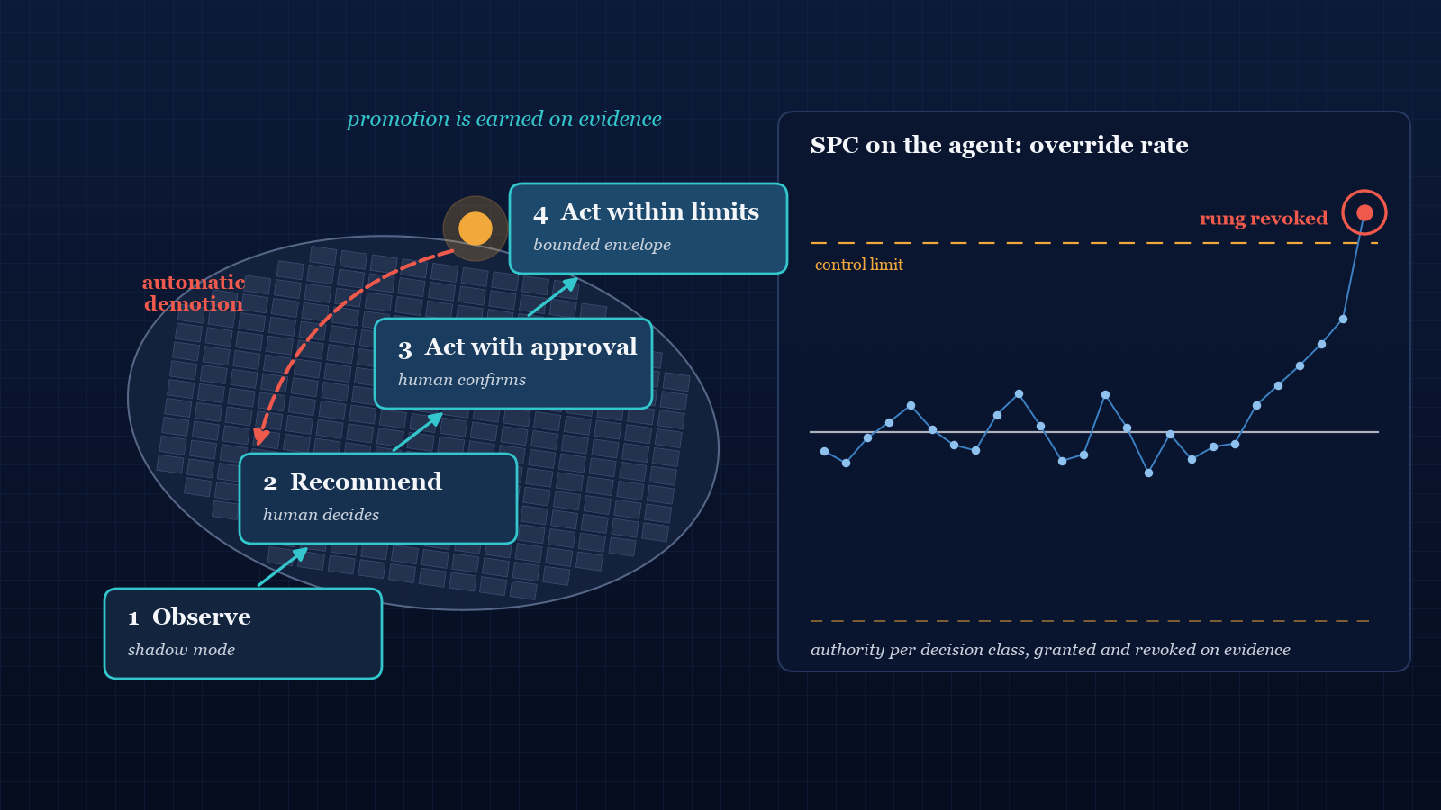
AI may close the design. The fab may finish the silicon. Production still has to realize the system.
Semiconductor engineering is becoming extraordinarily capable.
EDA platforms are expanding from individual design tasks toward increasingly complete system analysis.
Multiphysics simulation is connecting electrical, … Read More


Verification IP proves essential for PCIe GEN5