AI, hyperscale data centers, and data-intensive workloads are driving unprecedented demands for performance, bandwidth, and energy efficiency. As the economic returns of traditional transistor scaling diminish, advanced IC packaging and heterogeneous integration have become the primary levers for system-level scaling. Chiplet-based architectures now dominate this transition, enabling modular design and process optimization but introducing dramatic increases in system and package complexity.
Package pin counts have grown from fewer than 100,000 to tens of millions in leading-edge designs, with further growth expected. This complexity far exceeds what flat design methodologies or manual approaches can manage. System Technology Co-Optimization (STCO) has therefore emerged as a necessary framework for aligning architecture, silicon technology, and packaging. Hierarchical device planning provides the structural foundation required to make STCO effective at scale.
Recently, Siemens EDA published a whitepaper on this very topic and the following is a synthesized overview of that whitepaper. You can download the entire whitepaper from here.
Composable Systems: Reconfiguring 3D ICs for Early System Exploration
Modern systems are increasingly composed of multiple chiplets developed asynchronously and integrated using advanced 3D packaging technologies. While this composability improves flexibility and reuse, it makes early partitioning and integration decisions critical. Hierarchical device planning enables designers to assemble and de-assemble 3D IC systems early in the design process, allowing alternative partitioning, stacking, and interface strategies to be explored before physical commitments are made.
Although detailed layout information is unavailable at this stage, rapid approximate analyses enabled by hierarchical planning provide valuable insight into power integrity, signal integrity, thermal behavior, and mechanical risk. These early insights guide system exploration and prevent costly issues from becoming embedded in the design.
System Technology Co-Optimization (STCO) Begins at Package Planning
Packaging has become a primary determinant of system performance, power, cost, and reliability. Yet silicon design teams often lack early visibility into packaging constraints, leading to partitioning decisions that complicate integration. Hierarchical device planning addresses this gap by enabling fast creation of early package prototypes that support multi-domain analysis.
By generating preliminary bump maps, defining power and signal regions, and placing chiplets in 3D space, designers can evaluate packaging implications early and feed results back to silicon teams. This establishes a continuous, bidirectional feedback loop between architecture, silicon, and packaging, transforming STCO from a sequential handoff into a concurrent optimization process.
Taming Explosive Package Complexity with Hierarchical Planning
The exponential growth in package pin counts has rendered traditional flat planning approaches impractical. Managing millions of pins manually introduces unacceptable risk and inefficiency. Hierarchical device planning overcomes this challenge by decomposing complex package assemblies into structured, hierarchical elements such as chiplets, interfaces, and interconnect regions.
This hierarchical organization enables full-package connectivity tracking and verification across the entire 3D assembly. By providing structure and scalability, hierarchical planning allows designers to manage complexity without losing visibility or control.
Smart Pin Regions and Parametric Abstraction at Scale
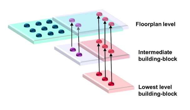
A key innovation of hierarchical device planning is the use of parameterized pin regions to abstract connectivity. Instead of defining individual pins, designers work with regions that encapsulate pin patterns, power and ground assignments, and interface characteristics. Pins are automatically synthesized from these parameters, ensuring consistency while dramatically reducing design effort.
CONNECTIVITY IN A HIERARCHICAL IC PACKAGE FLOORPLAN

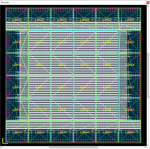
This parametric abstraction enables rapid iteration. Designers can adjust bump pitch, patterns, or net assignments and instantly regenerate connectivity, supporting fast design-space exploration and efficient response to changing requirements.
A DESIGN OF ARRAYED BLOCKS WITH PARAMETERIZED PINS

Cross-Domain Abstraction and Early Multi-Physics Insight
Effective STCO requires operating at the right abstraction level across electrical, thermal, mechanical, and manufacturing domains. Hierarchical device planning provides this abstraction while enabling early multi-physics analysis. Although early-stage analyses are approximate, they provide sufficient directional guidance to compare alternatives and identify high-risk design choices.
Integrated data management further supports this flow by ensuring consistency across rapidly evolving designs and preventing costly errors caused by outdated or mismatched data.
Summary
As semiconductor systems move toward increasingly heterogeneous and 3D-integrated architectures, managing complexity and cross-domain interaction becomes paramount. Hierarchical device planning enables early system assembly, scalable abstraction, and rapid multi-domain analysis, forming the foundation of effective System Technology Co-Optimization.
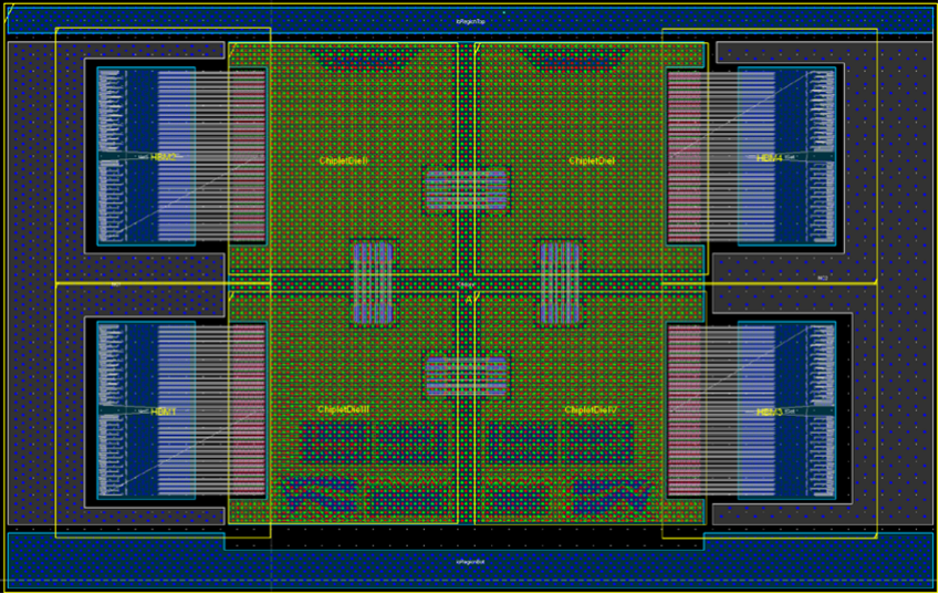
By enabling a shift-left design methodology and supporting informed decision-making when flexibility is highest and cost is lowest, hierarchical device planning transforms STCO into a practical, scalable engineering discipline for next-generation electronic systems.
A DESIGN COMPLETED USING HIERARCHICAL DEVICE PLANNING METHODOLOGY

You can download the entire whitepaper from here.
Also Read:
Siemens EDA Illuminates the Complexity of PCB Design
Siemens and NVIDIA Expand Partnership to Build the Industrial AI Operating System
Automotive Digital Twins Out of The Box and Real Time with PAVE360
Share this post via:


Comments
There are no comments yet.
You must register or log in to view/post comments.