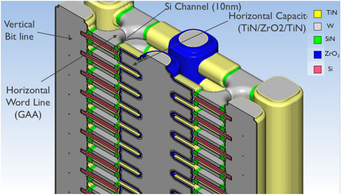
Epitaxial stacks of silicon and silicon germanium are emerging as a key materials platform for three dimensional dynamic random access memory. Future DRAM will likely migrate from vertical channels to horizontally stacked channels that resemble the gate all around concept in logic. That shift demands a starter material made of many repeating silicon and silicon germanium layers with sharp interfaces, precise thickness control, and a strain state that survives hundreds of repetitions. Meeting all three requirements at production scale on 300 millimeter wafers is the central challenge.
A representative target is a multi stack with at least one hundred bilayers. One practical recipe uses about sixty five nanometers of silicon and ten to fifteen nanometers of silicon germanium per period, with a germanium fraction near twenty percent. The higher germanium level is not arbitrary. It is chosen to enable a highly selective lateral removal of the silicon germanium during device patterning, which in turn opens space for the final silicon channels. The problem is that silicon and silicon germanium do not share the same lattice constant. The mismatch creates a constant drive to relax strain through misfit dislocations or through three dimensional island growth at elevated temperatures. Theory and prior experiments suggest that the total thickness of the silicon germanium far exceeds the critical limit for full relaxation, so success depends on suppressing every pathway that would let the lattice give way.
Material studies show that the inner portion of the wafer can remain fully strained even for stacks as large as one hundred twenty bilayers with ten nanometers of silicon germanium. Cross sectional transmission electron microscopy reveals two dimensional layer growth and smooth interfaces. Reciprocal space maps show vertically aligned satellite peaks, a signature of coherent strain, and energy dispersive x ray spectroscopy confirms composition uniformity from top to bottom. Achieving this result requires low growth temperature, extremely clean gases, and an oxide free starting surface so that the energy barrier to breaking bonds at the interface remains high.
Near the wafer rim the picture changes. The geometry at the bevel lowers the barrier for misfit formation, so dislocations appear at the edge even when the interior is perfect. The density of these edge defects grows with the number of bilayers and with the lattice mismatch. Two practical mitigations exist. One can reduce the germanium content, which directly lowers the mismatch. Alternatively one can co alloy the silicon germanium with a small amount of carbon, which produces a similar effect on the lattice parameter. Experiments show that both approaches reduce edge relaxation. Adding carbon also sharpens interfaces at the silicon on silicon germanium transition. However carbon has a limited solubility in the alloy, so there is a concentration beyond which crystalline quality begins to suffer.
Uniformity over time and across the wafer is the second pillar. Thick stacks exhibit a gradual drift in period thickness from bottom to top and a worsening of within wafer uniformity toward the edge. A key culprit is the thermal environment of the reactor. During long runs the quartz tube accumulates a film that absorbs lamp energy, warms the tube, and perturbs the gas temperature field. The result is a slow change in growth rate that maps into both layer to layer and lateral non uniformities. Tools that actively control the tube temperature reduce these drifts. Independent tuning of hydrogen carrier flow and the temperature profile can push the relative standard deviation of layer thickness to near one percent.
Chemistry choices matter as well. To keep interfaces sharp at moderate temperature, silicon germanium growth benefits from dichlorosilane and germane while the silicon layers use silane. The lower temperature suppresses silicon and germanium intermixing, as confirmed by secondary ion mass spectrometry, and reduces the risk of three dimensional islanding. At the same time the process must avoid amorphous or polycrystalline defects that can seed dislocations. Maintaining a chlorine passivated surface during step transitions helps remove early stage imperfections and keeps the surface ready for two dimensional growth.
The overall lesson is clear. Three dimensional DRAM is feasible with epitaxial silicon on silicon germanium stacks that reach one hundred or more periods, but only when growth conditions, reactor thermals, and alloy choices are co designed. The interior can be kept fully strained, the edge can be tamed by lowering mismatch, and the interfaces can remain sharp enough for selective etching. When these threads are woven together, materials science delivers a realistic foundation for the next DRAM architecture.
You can read the source article here.
Also Read:
Breaking out of the ivory tower: 3D IC thermal analysis for all
PDF Solutions and the Value of Fearless Creativity
Streamlining Functional Verification for Multi-Die and Chiplet Designs
Share this post via:


Musk’s Orbital Compute Vision: TERAFAB and the End of the Terrestrial Data Center