Also Known As: TSMC 2nm node
Developer: Taiwan Semiconductor Manufacturing Company (TSMC)
Node Class: Advanced logic semiconductor node
Technology Generation: 2 nanometer (2nm)
Status (as of 2025): Risk production in progress; volume production expected in late 2025 or 2026
Overview
The TSMC N2 process node marks a major milestone in semiconductor manufacturing by introducing Gate-All-Around Field-Effect Transistor (GAAFET) technology at scale. As the successor to TSMC’s N3 and N3E process families, N2 is the company’s first node to depart from FinFET transistors since their introduction in the 16nm generation.
N2 is designed to significantly boost performance, power efficiency, and transistor density, enabling next-generation compute platforms in AI, mobile, HPC, automotive, and 5G infrastructure. The N2 node is foundational to TSMC’s multi-node roadmap, competing directly with Intel 20A/18A and Samsung’s 2GAP (2nm-class) nodes.
Key Technical Features
1. GAAFET Transistor Architecture
-
N2 uses nanosheet-based GAAFETs, where the gate fully surrounds the channel, offering superior electrostatic control and reduced short-channel effects compared to FinFETs.
-
The width of the nanosheets can be adjusted (called “width quantization”) to fine-tune performance and leakage characteristics.
-
Benefits include:
-
Higher drive current per footprint.
-
Lower leakage current.
-
Better scalability to sub-2nm nodes.
-
2. Backside Power Delivery Network (BSPDN)
-
N2 is TSMC’s first node to introduce BSPDN—where power lines are routed under the transistor layer.
-
Advantages:
-
Reduced IR drop and power rail congestion.
-
Improved routing resources for signal interconnects on the frontside.
-
Boosts power efficiency and frequency scaling.
-
3. EUV Lithography Enhancement
-
N2 leverages enhanced EUV (Extreme Ultraviolet Lithography) for patterning critical layers with fewer multiple-patterning steps.
-
N2 likely uses High-NA EUV for some back-end or contact layers (depending on yield maturity).
-
EUV enables smaller features and lower edge-placement errors compared to DUV.
4. Advanced Interconnect Stack
-
Introduction of new barrier/liner materials and lower-k dielectrics.
-
Improvements in via resistance and trench RC delay.
-
Enhanced reliability and thermal stability for dense, high-power designs.
5. Design Technology Co-Optimization (DTCO)
-
N2 includes new standard cell libraries, SRAM compilers, and logic IP optimized for nanosheet GAA.
-
Co-optimization of transistor, interconnect, and power delivery enables better Performance-Per-Watt-Per-Area (PPPA) scaling.
Performance Targets (vs. N3E)
According to TSMC’s public statements:
| Metric | N3E (Baseline) | N2 (Target) |
|---|---|---|
| Performance | — | +10% to +15% |
| Power Efficiency | — | –25% to –30% |
| Logic Density | — | +10% to +20% |
| Transistor Type | FinFET | GAAFET (nanosheet) |
Note: Exact numbers depend on the implementation (e.g., HPC vs. mobile libraries).
Development Timeline
| Year | Milestone |
|---|---|
| 2021 | TSMC announces GAAFET-based N2 roadmap publicly. |
| 2022 | Early DTCO and transistor R&D; PDK alpha versions provided to select customers. |
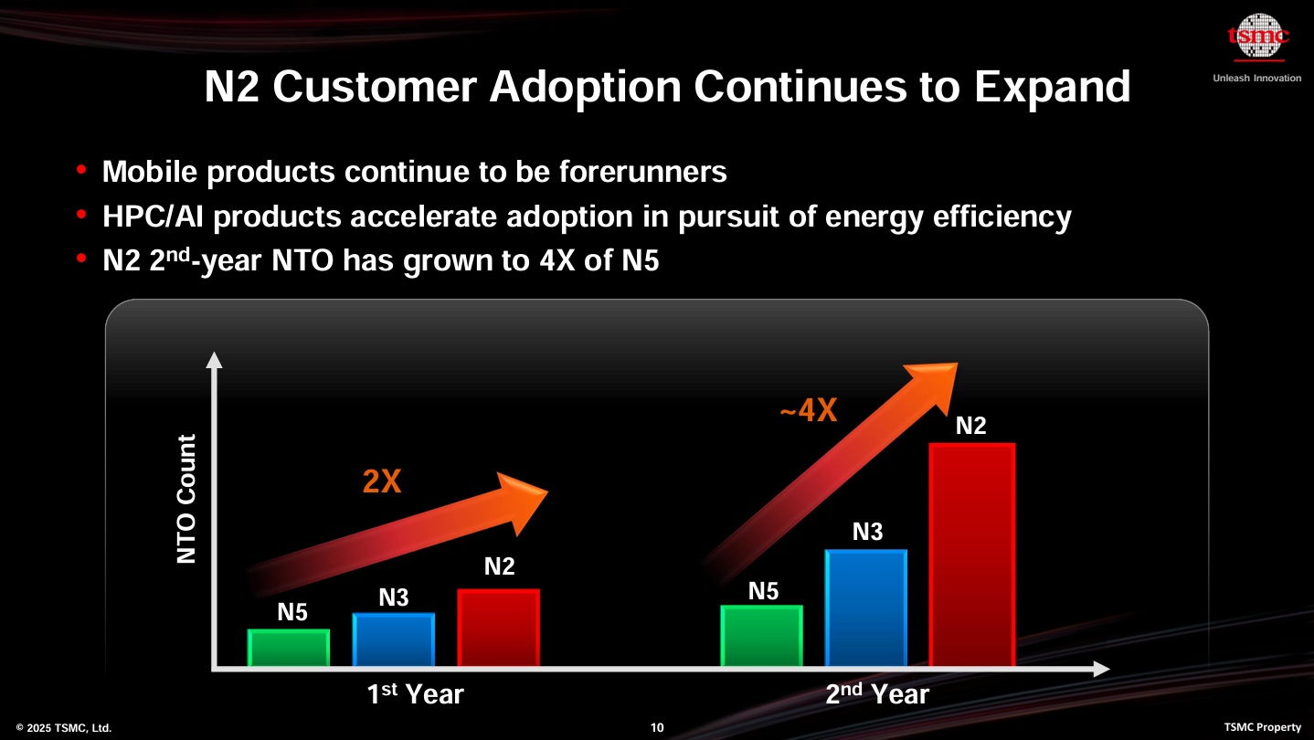
| 2023 | Risk production begins; early tapeouts from strategic customers (e.g., Apple, AMD, Nvidia). |
| 2024 | Pilot production; production equipment installation and yield learning ramp. |
| Late 2025 – 2026 | Volume production expected at Fab 20 (Baoshan) and Arizona (possibly late). |
| Post-2026 | Derivatives like N2P or N2X expected for enhanced performance and HPC use. |
Manufacturing Infrastructure
-
Primary Production Site: TSMC Fab 20 in Hsinchu Baoshan, Taiwan
-
Additional Capacity: Future N2-capable lines in Arizona Fab 21, depending on geopolitical and equipment readiness
-
Ecosystem Support: Broad PDK and EDA tool readiness from partners like Synopsys, Cadence, and Ansys by 2024
Applications and Use Cases
TSMC N2 is targeted for high-end chips in sectors that demand maximum performance and energy efficiency, including:
1. Mobile SoCs
-
Flagship processors from Apple, Qualcomm, MediaTek expected to adopt N2
-
Extended battery life and improved thermals for smartphones and tablets
2. High-Performance Computing (HPC)
-
CPUs and GPUs from AMD, Nvidia, and Intel (via IFS or joint ventures)
-
Improved AI acceleration and simulation performance
3. Artificial Intelligence (AI) Accelerators
-
Powering next-generation training and inference workloads
-
N2’s GAAFET and BSPDN features are well-suited for dense AI compute tiles
4. Automotive and Edge Devices
-
Functional safety and low leakage make N2 attractive for autonomous driving platforms and real-time sensor fusion processors
Challenges and Risks
-
Yield Ramp-Up: New GAA architecture and BSPDN require defect reduction and process stability.
-
Equipment Cost: Advanced EUV, backside metallization, and nanosheet processing demand expensive new tooling (e.g., High-NA EUV).
-
EDA and Design Flow Maturity: Adoption of GAAFET mandates updates to simulation, timing closure, and signoff tools.
-
Customer Cost: Increased wafer cost per mm² may limit N2 adoption to premium-tier chips initially.
Comparison to Competitors
| Foundry | Node | Transistor Type | Target Production | Notes |
|---|---|---|---|---|
| TSMC | N2 | GAAFET (nanosheet) | Late 2025–2026 | Industry leader; strong Apple/AMD pipeline |
| Intel Foundry | Intel 18A | RibbonFET (GAA), PowerVia | Late 2025-2026 | Potential leader in backside power and AI focus |
| Samsung Foundry | 2GAP | MBCFET (Samsung’s GAAFET) | 2025 (very limited) | First to GAA in 3nm, ramping slowly |
Future Evolution: Beyond N2
TSMC has hinted at multiple follow-on nodes:
-
N2P – Enhanced performance version, possibly with improved BSPDN and cell libraries.
-
N2X – High-performance variant for HPC with relaxed density scaling but higher drive current.
-
1.4nm and Beyond – Will continue nanosheet scaling; possible introduction of 2D materials, CFETs, or complementary GAA devices (p-n stacked).
Industry Impact
-
Solidifies TSMC’s lead in high-volume GAAFET manufacturing.
-
Sets new standard for power efficiency in mobile and AI compute.
-
Forces competitors to innovate aggressively in design, architecture, and packaging to match TSMC’s performance-per-watt edge.
-
Spurs massive ecosystem investment—from EDA vendors to OSATs—in nanosheet-compatible flows.
Conclusion
TSMC’s N2 process technology is a major leap forward in logic node scaling, driven by innovations in GAAFET transistors, backside power delivery, and advanced EUV integration. With risk production already in motion and volume production expected in 2025–2026, N2 will power the most advanced chips in the coming decade—fueling AI, edge, mobile, and HPC platforms with unprecedented efficiency and performance.
Share this post via:


Beyond Moore’s Law: High NA EUV Lithography Redefines Advanced Chip Manufacturing