![]()
Rapidus 2nm is Japan’s flagship next-generation logic process node, under development by Rapidus Corporation in collaboration with IBM and imec, targeting high-performance, energy-efficient, leading-edge semiconductor manufacturing. The goal is to achieve mass production readiness by 2027, marking Japan’s re-entry into the forefront of advanced logic manufacturing after decades of decline.
Built upon Gate-All-Around (GAA) nanosheet transistor architecture, the 2nm node represents a leap beyond FinFET scaling limits and is designed for applications in AI, HPC, automotive, and 6G communications.
Key Features
| Feature | Description |
|---|---|
| Transistor Type | GAA nanosheet (also known as Nanosheet FETs) |
| Gate Length | Sub-20nm, multi-stack sheets |
| Node Scaling | True 2nm-class dimensions based on metal pitch and contacted gate pitch |
| EUV Lithography | Uses extreme ultraviolet (EUV) lithography throughout the BEOL and FEOL |
| High Performance | Expected >45% performance gain compared to 7nm FinFET |
| Energy Efficiency | Estimated >75% power reduction at equivalent performance |
| Density | >2x transistor density improvement over 7nm |
| Backside Power Delivery (Planned) | Pathfinding for future node extensions, not first-gen |
Foundational Technology
Based on IBM 2nm Research Platform
-
Developed originally by IBM Research Albany (announced in 2021).
-
First public demonstration of stacked nanosheets with 12nm gate length.
-
Rapidus licensed IBM’s device architecture, process flow, and DTCO methodology.
imec Collaboration
-
Supports process integration, mask development, and material modeling through imec’s platform in Leuven, Belgium.
Timeline
| Year | Milestone |
|---|---|
| 2021 | IBM announces 2nm GAA prototype |
| 2022 | Rapidus founded and licenses IBM 2nm tech |
| 2023 | Construction of Chitose R&D fab begins |
| 2024 | EUV tools ordered, pathfinding with imec begins |
| 2025 | Pilot line operational in Hokkaido |
| 2026 | Process qualification |
| 2027 | Volume production of 2nm logic devices begins |
Technical Architecture
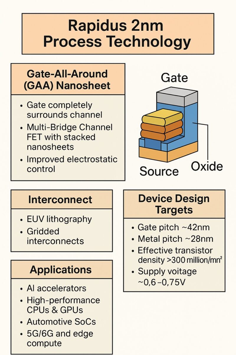
Gate-All-Around (GAA) Nanosheet
-
Multi-Bridge Channel FET structure: several nanosheets stacked vertically and fully surrounded by a gate.
-
Offers improved electrostatic control, lower leakage current, and greater scalability than FinFET.
-
Sheet width modulation enables tuning of performance and leakage tradeoffs.
Interconnect
-
EUV patterning with 1D gridded interconnects for tighter pitch.
-
Advanced middle-of-line process integration for signal routing.
Device Design Targets
| Metric | Target |
|---|---|
| Gate pitch | ~42nm |
| Metal pitch | ~28nm |
| Effective transistor density | >300 million/mm² |
| Supply voltage | ~0.6–0.75V |
| Frequency scaling | >4GHz design feasibility |
Applications
The Rapidus 2nm node is being designed for:
-
AI accelerators
-
High-Performance CPUs & GPUs
-
Automotive SoCs (ASIL-D target)
-
5G/6G and edge compute
-
Low-power mobile/embedded systems
Competitive Landscape
| Company | Node | Target Year |
|---|---|---|
| TSMC | N2 | 2025–2026 (risk prod), 2026–2027 (HVM) |
| Intel | Intel 20A / 18A | 2024 (pre-2nm, ribbonFET) |
| Samsung | SF2 / SF1.4 | 2025+ |
| Rapidus | 2nm | 2027 |
Although Rapidus trails TSMC and Samsung by 1–2 years in ramp, it is targeting a “leapfrog” approach through ecosystem co-development and tight design-technology co-optimization (DTCO) with global partners.
Challenges
| Area | Details |
|---|---|
| Workforce | Recruiting and training engineers for GAA and EUV is ongoing |
| Ecosystem | Japan lacks native EDA, IP, and 2nm tapeout flow vendors |
| Yield Ramp | High defect sensitivity due to small feature sizes |
| Capital Investment | 2nm fabs cost $15–20B; needs sustained government support |
Government Support
-
Supported by METI (Ministry of Economy, Trade and Industry)
-
Expected $5–10 billion in subsidies over multiple years
-
Aligned with Japan’s economic security and semiconductor sovereignty initiatives
Summary
The Rapidus 2nm process represents a bold national effort by Japan to re-enter the top tier of semiconductor manufacturing. With IBM’s GAA nanosheet platform, imec collaboration, and Japanese industrial strength, Rapidus seeks to become a trusted, high-performance foundry for advanced AI and compute semiconductors in the post-FinFET era.
Also Read:
Share this post via:


Silicon Insurance: Why eFPGA is Cheaper Than a Respin — and Why It Matters in the Intel 18A Era