Overview
Electronic Design Automation (EDA) refers to a category of software tools and methodologies used to design, verify, and manufacture integrated circuits (ICs), systems-on-chip (SoCs), FPGAs, and printed circuit boards (PCBs). EDA enables the complex process of converting electronic system specifications into functional, manufacturable silicon devices.
EDA is the foundation of modern semiconductor design, essential for creating chips at advanced nodes like 5nm, 3nm, and beyond. The EDA industry includes both commercial vendors (e.g., Synopsys, Cadence, Siemens EDA) and a growing open-source ecosystem.
EDA Flow Overview
EDA tools are typically organized into a structured design flow that spans multiple domains:
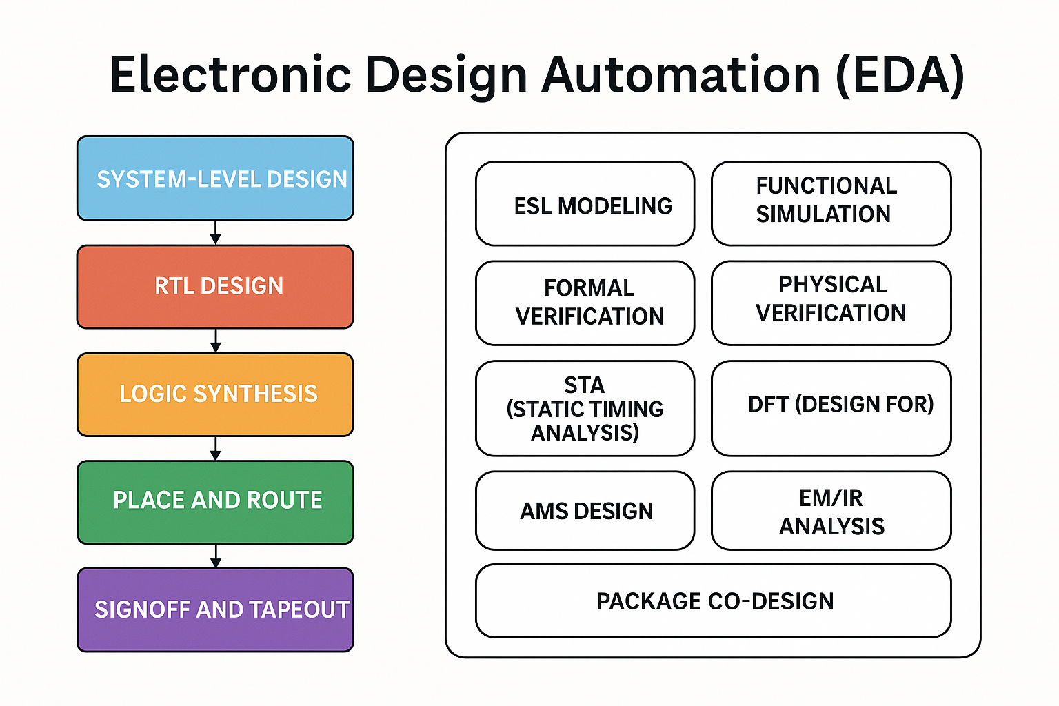
1. System-Level Design
-
Specification of high-level functionality
-
ESL (Electronic System Level) modeling
-
SystemC, TLM, C/C++, MATLAB
2. RTL Design
-
Register Transfer Level (RTL) coding in Verilog or VHDL
-
Defines the chip’s logic behavior
-
Functional simulation (e.g., using ModelSim, VCS)
3. Logic Synthesis
-
Converts RTL into gate-level netlist
-
Maps logic to standard cells
-
Tools: Synopsys Design Compiler, Cadence Genus
4. Formal Verification & Equivalence Checking
-
Ensures RTL and netlist are logically identical
-
Tools: Synopsys Formality, Cadence Conformal
5. Static Timing Analysis (STA)
-
Ensures timing constraints are met across all corners
-
Tools: PrimeTime (Synopsys), Tempus (Cadence)
6. Place and Route (Physical Implementation)
-
Physical placement of cells and routing interconnects
-
Power planning, clock tree synthesis (CTS), metal layers
-
Tools: Innovus (Cadence), Fusion Compiler (Synopsys), Aprisa (Siemens)
7. DFT (Design for Test)
-
Adds scan chains, BIST (Built-In Self-Test)
-
Ensures testability of manufactured silicon
8. Physical Verification
-
DRC (Design Rule Check)
-
LVS (Layout vs. Schematic)
-
Antenna checks, electromigration
-
Tools: Calibre (Siemens), Pegasus (Cadence)
9. Signoff & Tapeout
-
Final checks before delivering GDSII to foundry
-
PPA (Power, Performance, Area) optimization
-
Signoff tools: RedHawk (Ansys), Voltus (Cadence), PrimeTime SI (Synopsys)
Other Key Domains
| Domain | Description |
|---|---|
| Analog/Mixed-Signal (AMS) Design | Custom schematic/layout using tools like Virtuoso |
| FPGA Design | RTL → bitstream via Vivado, Quartus, Intel FPGA tools |
| PCB Design | Layout of boards using Altium, OrCAD, Xpedition |
| EM/IR Analysis | Power integrity, thermal modeling |
| Package Co-Design | IC/package/board electrical + thermal co-simulation |
Major EDA Companies
| Vendor | Key Tools / Strengths |
|---|---|
| Synopsys | Fusion Compiler, Design Compiler, PrimeTime, ARC processors |
| Cadence Design Systems | Innovus, Virtuoso, Spectre, Xcelium, Tensilica |
| Siemens EDA (ex-Mentor Graphics) | Calibre, Tessent, Aprisa, Xpedition |
| Ansys | RedHawk, Totem, power and thermal analysis |
| Keysight EDA | RF, microwave, signal integrity tools |
| Empyrean Technology | Analog/mixed-signal EDA (China) |
| Agnisys, Defacto, AMIQ, OneSpin, Axiomise | Niche providers in verification, design automation, and formal tools |
Market Size & Growth
-
EDA market size (2024): Estimated at $15–18 billion
-
Projected CAGR: ~9–10% through 2030
-
Drivers:
-
Explosion of AI/ML SoCs
-
Automotive (ADAS, autonomous driving)
-
3D ICs and chiplets
-
Advanced packaging and heterogeneous integration
-
Key Trends and Innovations
1. AI/ML in EDA
-
Tools increasingly use ML for:
-
Floorplanning
-
Timing prediction
-
Bug classification
-
-
Example: Synopsys DSO.ai, Cadence Cerebrus
2. Chiplet and 3D IC Design
-
Requires die-to-die PHY, interposer-aware floorplanning
-
TSMC 3DFabric, Intel Foveros, Samsung X-Cube
-
New tools for co-design across chip + package
3. Cloud-based EDA
-
Exploding simulation/verification workloads shift to cloud
-
EDA vendors offering cloud-native platforms
-
Synopsys Cloud, Cadence CloudBurst
-
4. Open Source EDA
-
Tools: Yosys, OpenROAD, Magic, KLayout, Verilator
-
Driven by RISC-V, academia, DARPA’s IDEA program
-
Growing traction for FPGA prototyping and chiplets
Security & Safety in EDA
| Topic | Tools/Practices |
|---|---|
| Hardware security | Trojans, backdoors, IP tampering |
| Formal verification | Ensures functional correctness |
| Functional Safety | ISO 26262 compliance for automotive |
| Supply Chain Protection | Traceability and anti-counterfeit checks |
| Quantum-Safe IP Integration | EDA support for PQ cryptography blocks |
Key Challenges
-
Design Complexity: Chips now have tens of billions of transistors
-
Time to Market: Shrinking due to consumer demand and competition
-
Process Variability: Increased modeling demands below 5nm
-
Verification Bottlenecks: 70%+ of effort goes into validation

Also see:
Cadence Design Systems, Inc. Wiki
Share this post via:


Chemical Origins of Environmental Modifications to MOR Lithographic Chemistry