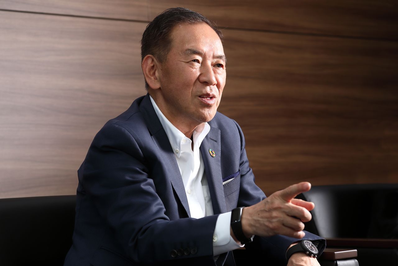
Dr. Atsuyoshi Koike is the President & CEO of Rapidus Corporation, Japan’s advanced-logic foundry initiative targeting commercialization of 2-nm gate-all-around (GAA) technology later this decade. A veteran of Japan’s semiconductor industry, Koike is known for linking bold process roadmaps with pragmatic factory discipline—especially his advocacy of single-wafer processing and fast learning loops in manufacturing.
“Speed of learning beats sheer scale.” — public remarks (translated)
Early life and education
Koike was born in Chiba Prefecture in 1952. He studied materials and electronic engineering, earning graduate degrees that grounded him in device physics, process technology, and yield optimization—training that later shaped his “process-first, iteration-fast” approach to leading-edge nodes.
Career highlights
-
Hitachi — Early engineering and management roles across device and manufacturing organizations.
-
Trecenti Technologies (300-mm fab) — President & CEO; championed single-wafer processing to tighten process control, reduce work-in-process latency, and accelerate yield learning.
-
SanDisk K.K. / Western Digital Japan — Country-level leadership spanning NAND supply, quality, and customer engagement at scale.
-
Renesas — Senior engineering leadership bridging product and manufacturing.
-
Rapidus (2022–present) — Founding CEO of Japan’s bid to return to the leading edge with 2-nm GAA logic and tightly integrated advanced packaging.
“My idea is single-wafer processing.” — on factory philosophy
Leadership philosophy
Koike’s leadership blends three pillars:
-
Rapid learning cycles. Run smaller lots, measure more, iterate faster.
-
Design–manufacturing co-optimization (DMCO). Tighten the loop between PDKs, EDA, design rules, and line-of-record process modules so chips and factories co-evolve.
-
Factory humanism. Build teams that can reason from first principles, not just follow recipes; train new talent alongside veterans to keep knowledge compounding.
“At the leading edge, yield is a knowledge problem before it is a volume problem.”
Rapidus strategy
-
Node focus. Leapfrog legacy FinFET and stand up GAA at 2-nm, aligning transistor architecture, patterning, and variability control with EUV-heavy flows.
-
Fab model. A greenfield site in Chitose, Hokkaidō (IIM-1) designed for short feedback loops—from tool trials to device splits to parametric sign-off—emphasizing controllability over sheer WSPM.
-
Packaging & chiplets. Build advanced packaging next to wafer lines (RDL interposers, 2.5D/3D) and publish Assembly Design Kits (ADKs) so customers can co-design systems across die boundaries.
-
Ecosystem. Partner with equipment, materials, and research leaders; cultivate a Hokkaidō-centered cluster spanning universities, suppliers, and design houses.
-
Customers. Target “medium-batch” high-performance products—AI, HPC, networking, and autonomy—where time-to-learning and customization matter as much as sheer output.
“We plan to supply customers with medium-batch needs.”
Technology themes
-
Single-wafer control. By processing wafers one at a time in critical steps, the fab can run denser experiments, catch excursions earlier, and converge faster on uniformity and defectivity.
-
Device variability. GAA brings strong electrostatics but a narrow process window; Koike emphasizes metrology-heavy bring-up and guard-banded patterning to tame threshold variability and line-edge roughness.
-
EUV maturity. Multi-layer EUV stacks demand relentless uptime, contamination control, and resist/process co-design—areas where disciplined fab ops set the pace.
-
Thermals, power, memory. System PPA increasingly lives in the package; Rapidus treats HBM attach, thermal path design, and die-to-die fabrics as first-class citizens.
“The package is part of the processor now.”
Talent, training, and culture
Koike frequently stresses the need to rebuild Japan’s deep manufacturing bench while attracting global experts. He argues for a “virtual university” model—curricula that traverse device physics, lithography, integration, DFM/DFY, advanced packaging, and operations—so new hires can become productive quickly.
“We must teach the full stack—from atoms to algorithms.”
Sustainability and power
Acknowledging the energy intensity of leading-edge fabs and AI systems, Koike frames sustainability as design constraint rather than marketing:
“Our third pillar is total commitment to greening—power, water, materials—engineered into the line from day one.”
Risks and execution challenges
-
Capital and cadence. Sustained funding through pilot, risk production, and volume ramp.
-
Yield & cycle time. Shrinking defectivity while keeping cycle times short enough to learn quickly.
-
Supply chain. Securing EUV/DUV capacity, advanced materials, masks, and HBM at scale.
-
Power & site. Building reliable, low-carbon power and utilities for a dense, EUV-heavy fab.
-
Customer conversion. Turning early interest into committed tape-outs aligned with the ramp window.
“Execution is the only narrative that matters.”
Legacy and significance
Koike positions Rapidus as both industrial policy and engineering experiment: can a nation re-enter the cutting edge by optimizing for speed, learning, and co-design rather than brute scale alone? If the answer is yes, Japan regains a durable role at the vanguard of logic; if not, the lessons on what it takes to compete at 2-nm will still shape the next generation of fabs, wherever they are built.
“Our mission is to develop, manufacture, and provide cutting-edge semiconductors made in Japan to the world.”


Silicon Insurance: Why eFPGA is Cheaper Than a Respin — and Why It Matters in the Intel 18A Era