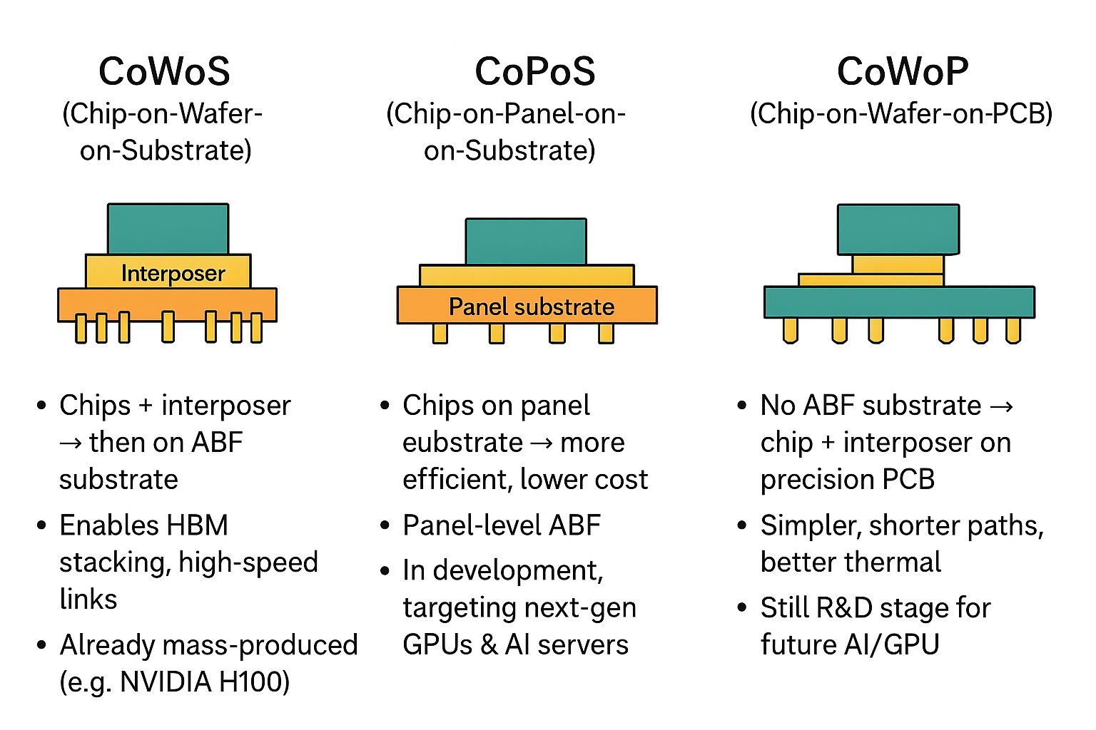


Chip-on-Wafer-on-PCB (CoWoPCB) is a heterogeneous integration flow in which bare dies (“chips”) are first assembled and interconnected at wafer scale (on an interposer or fan-out carrier). The completed wafer-level module is then finished with board-pitch I/O and mounted directly to a printed circuit board (PCB)—eliminating the traditional package substrate. The goal is to combine wafer-level density and short interconnects with PCB-level cost, area, and system modularity.
Typical targets include AI accelerator cards, networking line cards, high-bandwidth storage controllers, RF front-ends, and compact embedded compute modules where z-height, latency, and cost per function are critical.
Why CoWoPCB?
-
Substrate removal: Skips the package substrate to cut cost and stack height while reducing thermal interfaces.
-
Wafer-level density: Chiplets, SRAM tiles, and HBM/base dies can be joined at fine pitch (micro-bump or hybrid bond).
-
Board-level modularity: The module becomes a directly solderable (or socketable) “system brick,” simplifying mechanics and inventory.
-
Latency & power: Shorter interconnects from logic↔memory and logic↔I/O reduce RC delay and I/O power.
Architecture & Building Blocks
-
Wafer-level carrier
-
Silicon interposer with TSVs for extreme wiring density and skew control.
-
Fan-out RDL-on-wafer (TSV-less) for low z-height and cost efficiency.
-
Glass wafer carriers (emerging) for improved dimensional stability and low loss; TGVs optional.
-
-
Die attach & interconnect
-
Micro-bump pitches from ~45 μm trending to ≤20 μm; hybrid bonding ≤10 μm for ultra-low resistance/capacitance.
-
-
Board-pitch interface
-
Wafer-side RDL hierarchy that fans out from micron-scale wiring to BGA/LGA suitable for PCB assembly (e.g., 0.5–1.0 mm ball pitch, design-dependent).
-
Underfill, corner staking, or compliant interposers for solder-joint reliability.
-
-
Thermo-mechanical elements
-
Stiffeners/frames, lids, vapor chambers or cold plates; optional cavity PCBs for co-planarity and z-height control.
-
Representative Process Flow
-
Carrier fabrication (wafer level): Build TSV/TGV (if used), multilayer RDL, and UBM on silicon/glass/fan-out carrier.
-
Chip attach (wafer level): Place logic tiles, HBM stacks (or HBM base dies), analog/RF chiplets; micro-bump or hybrid bond; apply NCF/MUF; cure and clean.
-
Wafer thinning & finish: Back-grind/polish; add backside RDL/PDN; probe for known-good-module where feasible.
-
Board-pitch I/O formation: Build bump/land arrays (BGA/LGA) and protective structures on the wafer module’s underside to meet PCB assembly rules.
-
Singulation: Dice the wafer into modules; add lids/stiffeners/thermal hardware as required.
-
Board assembly: SMT attach module directly to PCB; underfill/stake as needed; attach heat spreaders/cold plates; system-level test.
Flows may be “chip-first” or “RDL-first,” and board attach can be solder reflow, thermocompression with adhesives/films, or LGA + compression frame.
Design & Integration Considerations
-
PDN co-design: Stack-up must bridge wafer planes to PCB planes with low inductance paths; consider hierarchical decoupling (on-wafer MIM, interposer planes, board VRM proximity).
-
Signal integrity: Ultra-wide HBM buses and die-to-die fabrics demand controlled impedance, short stubs, back-drilled vias, and low-loss board dielectrics.
-
Thermals: High-TDP modules (>300 W possible) require direct-attach lids, high-k TIMs, and board-level cooling hardware. Thermal gradients drive mechanical stress—simulate early.
-
CTE mismatch: Silicon ↔ FR-4/low-CTE laminates need compliant joints, underfill, and symmetric build-ups to manage fatigue and warpage.
-
Test strategy: Invest in KGD; add wafer-module test pads and PCB boundary-scan/JTAG access; plan for system-in-test (SiT) vectors and on-board monitors.
Variants You’ll Hear About
-
CoWoPCB-Si: Silicon interposer at wafer level, direct BGA to PCB. Max density and performance.
-
CoWoPCB-RDL: TSV-less fan-out carrier; thinnest z-height, attractive cost/performance.
-
CoWoPCB-Glass: Glass carrier and/or glass-core PCB for flatness and low loss (ecosystem maturing).
-
Cavity CoWoPCB: Module recessed into a PCB cavity for mechanical support and lower profile.
-
Socketed CoWoPCB: LGA compression or mezzanine connector for field-replaceable modules.
CoWoPCB vs. Other Approaches (quick take)
-
vs CoWoS: Removes the package substrate; relies on wafer-side fan-out to reach board pitch, trading some routing freedom for lower cost/z-height.
-
vs Fan-Out Panel-Level Packaging (FO-PLP): FO-PLP embeds dies in mold on a panel; CoWoPCB leverages wafer-level precision and then goes straight to PCB, benefiting modules that need extreme intra-module density.
-
vs EMIB/bridge substrates: Bridges excel inside a package substrate; CoWoPCB externalizes the module to the PCB, simplifying system assembly at the expense of some substrate-level routing options.
-
vs Package-on-Package (PoP) / SiP: CoWoPCB targets board integration directly, favoring large, high-power modules and aggressive thermals.
Prime Use Cases
-
AI/HPC accelerator modules: Multi-tile logic + 6–12× HBM with short, dense channels and board-level cooling.
-
Switch/Router ASICs: High-lane-count SerDes, co-packaged optics adjacency on the board.
-
Edge/embedded compute: Thin modules in cavity PCBs for robotics, avionics, and telecom.
-
RF/mixed-signal front-ends: Short path to antennas/filters on the board while keeping analog dies close together on wafer.
Manufacturing & Ecosystem
-
Foundry/OSAT alignment: Interposer and wafer-level assembly must align with PCB fab/assembly DFM, including stencil, paste, profile, and co-planarity specs.
-
PCB partners: Low-loss, high-Tg, low-CTE laminates; blind/buried vias, via-in-pad and back-drill capability; tight impedance control.
-
Equipment & materials: Large-format bonders, precise warpage control fixtures, robust underfills, high-reliability solder alloys, advanced TIMs and lids.
Key Challenges
-
Board-level reliability: Solder-joint fatigue under thermal cycling and vibration; mitigated via underfill, corner staking, and compliant interposers.
-
Warpage budgets: Module flatness across reflow; manage through symmetric build-ups, frames, cavity boards, and tuned profiles.
-
I/O fan-out: Bridging from ≤10 μm wafer wiring to 500–1000 μm board pitch without crosstalk or IR drop penalties.
-
Reworkability: Direct-attach modules are harder to rework than socketed cards; design service strategies accordingly.
-
Test coverage: Ensuring high coverage before permanent board attach; plan for board-level diagnostics and field telemetry.
Roadmap & Metrics to Watch
-
Hybrid-bond adoption: Moving chiplet and memory base-die joins to ≤10 μm mainstream.
-
RDL scaling: Stable 1–2 μm L/S on wafer carriers plus robust board-pitch transition stacks.
-
Low-CTE boards: Wider availability of low-CTE glass/organic cores to reduce solder strain.
-
Thermal density: Module-level heat flux targets and standardization of liquid-cool plate interfaces.
-
Yield orchestration: Known-good-die, known-good-module, and board-level screening to control compounded yield loss.
Practical Design Tips
-
Partition chiplets to keep the noisiest fabrics closest and shortest; isolate analog/RF islands with guard structures at the wafer level.
-
Use hierarchical PDN: on-wafer MIM caps, interposer planes, then thick board planes with local VRMs.
-
Add sacrificial test pads on the wafer module and boundary-scan hooks on the PCB for bring-up and field debug.
-
Co-design thermals and mechanics early: lid selection, clamp points, cavity depth, and keep-outs for cold-plate plumbing.
-
Specify board fab rules that match your BGA escape and back-drill assumptions; validate in 3D EM/thermal-mechanical sims.
Notable Quotes (unattributed)
-
“If you can wire it at wafer pitch and land it at board pitch, you’ve built a bridge from physics to economics.”
-
“CoWoPCB turns packaging into a system module, not just a protective shell.”
-
“Eliminate the substrate and you remove a cost layer and a thermal interface—but only if reliability keeps up.”
-
“Board attach makes test strategy a first-class citizen; what you don’t catch before reflow becomes a field problem.”
-
“In the chiplet era, PDN integrity is the new floorplan.”
-
“Glass brings flatness; design brings yield.”
-
“Short wires save watts; good mechanics save products.”
Glossary
-
Interposer: Dense wiring layer (often silicon) that connects multiple chiplets at fine pitch; may use TSVs.
-
RDL (Redistribution Layer): Thin-film metallization that reroutes I/O to different pitches/locations.
-
Hybrid Bonding: Cu-to-Cu and dielectric direct bonding enabling ultra-fine pitch interconnects with low resistance.
-
BGA/LGA: Ball-grid or land-grid array interfaces suitable for standard PCB assembly or compression sockets.
-
CTE (Coefficient of Thermal Expansion): Mismatch between materials that drives stress during temperature changes.
-
Cavity PCB: Board with a recessed pocket to host a module, improving planarity and reducing z-height.
Also Read:
Share this post via:


Things From Intel 10K That Make You Go …. Hmmmm