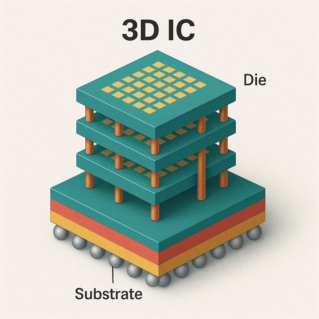

A 3D Integrated Circuit (3D IC) is a device in which two or more active electronic layers (dies or wafers) are vertically stacked and interconnected to function as a single integrated system. These layers are interconnected using fine-pitch vertical interconnects, such as Through-Silicon Vias (TSVs) or hybrid bonds, allowing high bandwidth, reduced power, and smaller form factors.
Background and Evolution
As semiconductor devices approached the physical limits of Moore’s Law, shrinking transistors became economically and technologically more difficult. At the same time, demand surged for higher memory bandwidth, lower latency, and heterogeneous compute. This shift drove research into “More-than-Moore” strategies like 3D integration.
Timeline
-
2000s: Research phase; DARPA, IMEC, and IBM lead initial 3D stacking projects.
-
2010–2014: Hynix and Samsung deploy HBM1/2 with TSVs in memory.
-
2015–2020: AMD develops 3D chiplet architectures; Intel debuts Foveros.
-
2021–present: Hybrid bonding matures; TSMC rolls out SoIC, NVIDIA adopts HBM3, AMD 3D V-Cache launches.
Technology Stack: Types of 3D Integration
1. Die-to-Die (D2D)
-
Multiple known good dies (KGD) are stacked and connected via microbumps or hybrid bonds.
-
Popular in logic-memory pairings (e.g., SRAM-on-CPU).
2. Wafer-to-Wafer (W2W)
-
Two full wafers are aligned and bonded before singulation.
-
Higher density but lower yield due to wafer-level defects.
3. Die-to-Wafer (D2W)
-
Pre-tested dies are mounted on a target wafer.
-
Improves yield, supports heterogeneity.
Key Enabling Technologies
Through-Silicon Vias (TSVs)
-
Vertical vias drilled and filled with copper through silicon.
-
Used in memory stacks (HBM, 3D DRAM) and logic-memory hybrids.
-
Adds complexity: requires wafer thinning, TSV reveal, and isolation.
Hybrid Bonding
-
Next-gen alternative to microbumps.
-
Offers <10µm interconnect pitch, lower parasitics, and higher I/O density.
-
Examples: TSMC SoIC, Intel Foveros Direct.
Microbumps
-
Tiny solder balls (~20–50 µm) used for fine-pitch connections.
-
Used in older 3D stacking and 2.5D designs.
Wafer Thinning
-
Required for TSV exposure.
-
Final die thickness can be <50 µm in advanced packages.
Interposers (2.5D)
-
Passive or active silicon/organic substrates for lateral die connection.
-
Silicon interposers allow high-speed signaling between chiplets.
3D IC vs. 2.5D vs. Monolithic 3D
| Feature | 3D IC | 2.5D IC | Monolithic 3D |
|---|---|---|---|
| Structure | Dies stacked vertically | Dies placed side-by-side on interposer | Multiple layers built sequentially on same wafer |
| Vertical Interconnect | TSVs, Hybrid Bonds | Interposer routing | Local inter-layer vias |
| Cost | High | Medium | Very High |
| Maturity | Commercial | Widely adopted | Early R&D |
Design and Architecture Challenges
1. Thermal Management
-
Vertical stacking increases thermal density.
-
Solutions: heat spreaders, thermal TSVs, microfluidic cooling.
2. Power Delivery
-
Must supply each die stack efficiently.
-
Requires co-optimized PDNs and vertical power TSVs.
3. Signal Integrity
-
3D stacks introduce signal skew and noise.
-
Cross-layer timing closure and SI/PI analysis needed.
4. Testing and Yield
-
Limited test access post-stack; needs built-in self-test (BIST) or known-good-die flows.
-
Yield loss in one layer affects the entire stack.
5. Design Tools and IP
-
Requires EDA tools capable of 3D-aware floorplanning, thermal simulation, and TSV optimization.
-
IPs need to be retargeted or partitioned for 3D topologies.
Use Cases and Applications
1. High Bandwidth Memory (HBM)
-
3D-stacked DRAM over a logic base die.
-
Attached to GPUs, FPGAs, AI accelerators.
-
Standards: HBM2, HBM2E, HBM3, HBM3E (JEDEC).
2. CPUs and GPUs
-
AMD 3D V-Cache: L3 SRAM stacked on Ryzen cores for gaming and HPC.
-
Intel Meteor Lake: 3D-stacked logic using Foveros.
3. FPGAs
-
Xilinx and Intel use 3D and 2.5D integration for programmable logic and embedded memory.
4. AI and Machine Learning
-
NVIDIA H100, Cerebras, Tenstorrent utilize 3D packaging with HBM.
-
Enables massive memory bandwidth for training LLMs.
5. Aerospace and Defense
-
Space-constrained systems like satellites, where size, weight, and power (SWaP) are critical.
Major Companies and Technologies
| Company | 3D Technology | Key Products |
|---|---|---|
| AMD | 3D V-Cache, CoWoS | Ryzen 5800X3D, EPYC |
| Intel | Foveros, Foveros Direct | Meteor Lake, Ponte Vecchio |
| TSMC | SoIC, CoWoS, InFO | NVIDIA H100, AI chips |
| Samsung | X-Cube, H-Cube | HBM, SoC stacks |
| SK hynix / Micron | HBM3E, 3D DRAM | AI accelerators |
| ASE / Amkor | 3D/2.5D packaging | Commercial assembly |
Standards and Ecosystem
-
JEDEC: Defines standards like HBM and 3D DRAM.
-
IEEE 3D IC Conferences: Forum for academic and industrial R&D.
-
Open Compute Project (OCP): Driving chiplet and interconnect standardization.
-
UCIe (Universal Chiplet Interconnect Express): A standard for die-to-die links across 2.5D/3D systems.
Research Frontiers
-
Monolithic 3D ICs: Layer-by-layer transistor stacking for ultra-high density.
-
AI-driven EDA for 3D: Automating partitioning, thermal analysis, and TSV insertion.
-
Glass Interposers: Replacing silicon interposers for better thermals and lower cost.
-
Neuromorphic 3D Architectures: 3D memristors + compute layers for brain-like AI.
Economic and Market Impact
-
3D IC is essential to continuing performance-per-watt improvements.
-
Key to advanced AI chips and future data center architectures.
-
Enables more localized manufacturing, thanks to modular design and outsourced chiplets.
-
Drives chiplet economy, where small vendors can specialize in IP for 3D assembly.
Trivia and Fun Facts
-
AMD’s 3D V-Cache added 64MB of L3 on top of existing cores with minimal power penalty.
-
NVIDIA’s Grace Hopper uses 3D packaging for CPU-GPU interconnect with HBM.
-
The earliest DARPA-funded 3D IC work dates back to the 1980s, but it took 30+ years to commercialize.
-
Hybrid bonding allows TSV-less vertical stacking with <1µm alignment accuracy.

Also Read:
IC Packaging Comparison Wiki (TSMC, Intel, Samsung)
CoWoS® (Chip-on-Wafer-on-Substrate) Wiki
Share this post via:


Captain America: Can Elon Musk Save America’s Chip Manufacturing Industry?