At the pre-conference briefing, Dr. Kevin Zhang gave quite a few of us media types an overview of what will be highlighted at the 2025 TSMC Technical Symposium here in Silicon Valley. Since most of the semiconductor media are not local this was a very nice thing to do. I will be at the conference and will write more tomorrow after the event. TSMC was also kind enough to share Kevin’s slides with us.
The important thing to note is that TSMC is VERY customer driven so this presentation is based on interactions with the largest semiconductor manufacturing customer base the industry has ever seen, absolutely.
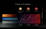
As you can imagine, AI is driving the semiconductor industry now not unlike what smartphones did for the last two decades. The difference being that AI consumes leading edge silicon at an alarming rate which is a good thing for the semiconductor industry. While AI is very performance centric, it must also be power sensitive. This puts TSMC in a very strong position from all of those years of manufacturing mobile SOCs for smartphones and other battery operated devices.
Kevin started with the AI revolution and how AI will be infused into most every electronic device from the cloud to the edge and will enable many new applications. Personally, I think AI will transform the world in a similar fashion as smartphones have but on a much grander scale.
Not long ago the mention of the semiconductor industry hitting $1T seemed like a dream. It is one thing for industry observers like myself to say it but it is quite another when TSMC does. There is little doubt in my mind that it will happen based on my observations inside the semiconductor ecosystem.
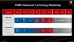
There have been some minor changes to the TSMC roadmap. It has been extended out to 2028 adding N3C and A14. The C is a compressed version meaning the yield learning curve is at a point where the process can be further optimized for density.
A14 will certainly be a big topic of discussion at the event. A14 is TSMC’s second generation of nanosheet transistor which is considered a full node (PPA) versus N2: 10-15% speed improvement at the same power, 25-30% power reduction at the same speed, and 1.2X logic density improvement. The first iteration of 14A does not have backside power delivery. It was the same with N2 which was followed by A16 with Super Power Rail (SPR). SPR for A14 is expected in 2029.
The TSMC 16A specs were updated as well. 16A is the first version of SPR for reduced IR drop and improved logic density. This has the transistor connection on the back. SPR is targeted at AI/HPC designs with improved signal routing and power delivery. A16 is on track for production in the second half of 2026. In comparison to N2P, A16 provides an 8-10% speed improvement at the same power, 15-20% power reduction at the same speed.
From what I have heard TSMC N2 is yielding quite well and is on track for production later this year. The big question is who will be the first customer to ship N2 product? Usually it is Apple but word on the street is the iPhones this year will again be using N3. I already have an N3 iPhone so I will skip this generation if that is the case. If Apple does an N2 based iPhone Max Pro this year then count me in!
TSMC N2P is also on track for production in the second half of 2026. As compared to N3E, N2P offers: 18% speed improvement at the same power, a 36% power reduction at the same speed, and a 1.2x density improvement.
The most interesting thing about N2 is the rapid growth of tape-outs between N5, N3, and N2. It really is astounding. Given that TSMC N3 was an absolute landslide for customer tape-outs I had serious doubts if we would ever see a repeat of that success but here we are. Again, in the past mobile was the driver for early tape-outs but now we have AI/HPC as well.
Finally, as Kevin said, TSMC N3 is the last and best FinFET technology available on such a massive scale with N3, N3E, N3P, N3X, N3A, and now N3C. Yet, N2 tape-outs beat N3 in the first year and the second year even more so. Simply amazing. I guess the question is who is NOT using TSMC N2?
The second part of the presentation was on packaging which will be covered in another blog. After the event I can provide even more details and get a feeling for the vibe at the event from the ecosystem. Exciting times!
UPDATE: TSMC is sharing recordings of the presentations HERE.
Also Read:
TSMC Brings Packaging Center Stage with Silicon
IEDM 2025 – TSMC 2nm Process Disclosure – How Does it Measure Up?
TSMC Unveils the World’s Most Advanced Logic Technology at IEDM
IEDM Opens with a Big Picture Keynote from TSMC’s Yuh-Jier Mii