Dr. Maksym Plakhotnyuk, is the CEO and Founder of ATLANT 3D, a pioneering deep-tech company at the forefront of innovation, developing the world’s most advanced atomic-scale manufacturing platform. Maksym is the inventor of the first-ever atomic layer advanced manufacturing technology, enabling atomic-precision development of materials, devices, and microsystems. A scientist with a Ph.D. in Nanotechnology, he has deep expertise in nanotechnologies, renewable and exponential technologies, semiconductor processing, solid-state physics, and material science. A Fulbright scholar, Hello Tomorrow Grand Winner, and proud Ukrainian, Maksym has earned global recognition for his work.
Tell us about your company?
One day, it dawned on me how tired I was of sitting in a cleanroom! I began to wonder – why is there no atomic printer for semiconductor materials, which would allow us to directly print materials atom by atom without the need for multiple steps, masks and cleanrooms? It took a small village but we eventually created our micronozzle that can construct custom designs in this way. This was the culmination of work between myself and my key partners, Ivan Kundrata (a machine engineering expert) and Prof. Julien Bachmann (a chemistry expert), and ATLANT 3D came to fruition in 2018.
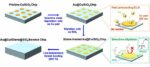
Today, ATLANT 3D is accelerating materials discovery by building materials and devices, atom by atom, through its direct atomic layer processing (DALP®) technology, which places precise amounts of materials exactly where needed. In a single step, the system creates complex structures for microelectronics, semiconductors, and advanced devices.
What problems are you solving?
By replacing traditional multi-step fabrication with direct atomic-scale manufacturing, this approach eliminates process complexity while reducing material waste by 90 percent. Research teams use DALP® technology to create what was previously impractical or impossible, from quantum computing components to devices that will operate in space. Our approach accelerates innovation across sectors by speeding up materials discovery while delivering a greener process.
What application areas are your strongest?
Our strongest application areas are materials innovation, advanced packaging for semiconductor manufacturing and AI, space exploration, optics and quantum computing. We are also increasingly targeting several sectors such as automotive, semiconductors, AI, communication and aerospace.
What keeps your customers up at night?
What keeps them up at night is wondering what they can accomplish with our technology. Materials discovery, or the process of finding new materials or discovering new applications for existing materials, is where we specialize, and it’s a very exciting space. Magic happens every day and the possibilities are endless!
What does the competitive landscape look like and how do you differentiate?
As discussed above, our approach accelerates innovation across sectors by speeding up materials discovery while delivering a greener process. With global demand for semiconductors showing no signs of abating, the industry remains somewhat of a paradox. On the one hand, semiconductors are vital to cutting-edge eco-friendly developments like electric cars and environmental sensors. But on the other, the current impact of the manufacturing process on the environment, and the size of its ecological footprint, are untenable. Approaches like ATLANT 3D’s are uniquely designed to help reconcile this, once and for all.
Another one of our strategic differentiators worth highlighting is the fact that we offer a platform for natural resilience. Since President Trump highlighted the need for a robust domestic semiconductor manufacturing ecosystem during his first term, there have been more than 100 new semiconductor projects announced across 28 U.S. states. The U.S. is now on track to triple its chip manufacturing capacity by 2032 and command a sizable share of the world’s advanced chip production.
But winning the chip race worldwide will not be easy, and the U.S. must continue to bolster domestic chip production and advance innovation. We’re on the precipice of a major revolution in semiconductor manufacturing and companies like ATLANT 3D are leading the charge.
ATLANT 3D’s approach supports more semiconductor manufacturing in the U.S. because it moves away from the model of heavily offshoring production to a small handful of multi-billion dollar foundries, to leveraging universities, startups and industrial R&D based domestically to dramatically accelerate discovery and the entire lab-to-fab process, while keeping costs in check. By creating a platform for U.S. strategic resilience, ATLANT 3D is helping to reduce our country’s dependency on foreign supply chains by delivering a modular platform that supports research, prototyping, and manufacturing. Universities, startups, and industrial R&D firms across the U.S. can integrate our technology immediately into their existing architectures.
What new features/technology are you working on?
Space exploration is a big focus area for us, and we’re working on the first space-compatible version of our technology that works in zero-gravity environments. In late 2023, ATLANT 3D announced a collaboration with the European Space Agency (ESA) to enable on-demand production of next-generation devices, microelectronics, and more in space. The goal was to make on-demand repair, maintenance, and manufacturing of high-precision components while in orbit possible, in the microgravity and zero-gravity environment of space.
In March 2025 – about sixteen months later – ATLANT 3D and ESA announced they achieved a key milestone in their collaboration, a version of ATLANT 3D’s atomic layer deposition (ALD) system that can function in a real-world space deployment, called the NANOFABRICATOR ZERO-G System (zero G stands for “zero gravity”). Ultimately, this marks an important step towards fully autonomous deep space exploration and inhabitation, including the Moon and Mars. Next steps for ATLANT 3D include further technology validation, commercialization and partnerships – expanding collaborations with space agencies and private companies for integration into future missions.
How do customers normally engage with your company?
We work with customers in a variety of different models, including joint projects with R&D players, original equipment manufacturer (OEM), original design manufacturing (ODM) and joint development equipment development arrangements.
Also Read:
CEO Interview with Carlos Pardo of KD