webinar banner AI 2026 v2

Semiconductors Up Over 20% in 2025

Semiconductors Up Over 20% in 2025
by Bill Jewell on 11-19-2025 at 2:00 pm

Semiconductors Up Over 20% in 2025 3

The world semiconductor market was $208 billion in third-quarter 2025, according to WSTS. This marks the first time the market has been above $200 billion. 3Q 2025 was up 15.8% from 2Q 2025, the highest quarter-to-quarter growth since 19.9% in 2Q 2009. 3Q 2025 was up 25.1% from 3Q 2024, the highest growth versus a year earlier since 28.3% in 4Q 2021.

The table below shows the top twenty semiconductor companies by revenue. The list includes companies which sell devices on the open market. This excludes foundry companies such as TSMC and companies which only produce semiconductors for their internal use such as Apple. The revenue in most cases is for the total company, which may include some non-semiconductor revenue. In cases where revenue is broken out separately, semiconductor revenue is used.

Nvidia remained the dominant number one supplier, with $57.0 billion in revenue. Korean memory companies Samsung and SK Hynix were two and three at $23.9 billion and $17.6 billion, respectively. Memory companies reported robust 3Q 2025 growth from 2Q 2025 with Kioxia up 31%, Micron Technology up 22%, Sandisk up 21%, Samsung up 19%, and SK Hynix up 10%. The strongest quarter-to-quarter growth rates among the non-memory companies were Sony Imaging at 51%, Nvidia at 22%, AMD at 20%, Broadcom at 16% and STMicroelectronics at 15%. MediaTek was the only company to report a revenue decline in 3Q 2025 of -5.5%.

Semiconductor company guidance for 4Q 2025 revenue change is mixed. Of the fourteen companies providing guidance, nine expect increasing revenue ranging from 14% at Nvidia to 1.4% at Renesas Electronics. Five companies guided revenue declines, ranging from -1.3% at Onsemi to -9.2% at Sony Imaging.

AI continues to drive semiconductor market growth with all the memory companies citing AI memory for data centers as the strongest growth area. Nvidia and AMD also attributed most of their growth to AI. Qualcomm and MediaTek are seeing growth in mobile handsets. The automotive segment is seen as generally flat, with some companies adjusting inventories.

Through the first three quarters of 2025, the semiconductor market is up 21.2% from a year ago, according to WSTS data. The market is much stronger than anticipated earlier in the year. The AI market has been booming in 2025, with Nvidia revenues for the first three quarters of 2025 up 62% from a year earlier. The major memory companies have cited AI as their major growth driver and are up 21% over the same time period.

Earlier in the year, many industry analysts (including us at Semiconductor Intelligence) were concerned about the effect Trump administration tariffs would have on the semiconductor market. However, the final tariffs were not as severe as expected and largely exempted semiconductors and electronic products.

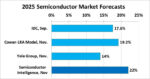
Recent forecasts for the 2025 semiconductor market growth range from 14% from Yole Group to 22% from us at Semiconductor Intelligence.

We at Semiconductor Intelligence have not finalized our 2026 semiconductor forecast. Current economic uncertainty will carry over into 2026. The semiconductor market has been overdependent on AI for growth in 2025 and this sector could moderate in 2026. Other sectors which have been weak in 2025 – such as PCs, smartphones and automotive – could see stronger growth in 2026. Our preliminary projection for 2026 is growth in the 12% to 18% range.

Semiconductor Intelligence is a consulting firm providing market analysis, market insights and company analysis for anyone involved in the semiconductor industry – manufacturers, designers, foundries, suppliers, users or investors. Please contact me if you would like further information.

Bill Jewell
Semiconductor Intelligence, LLC
billjewell@sc-iq.com

Also Read:

U.S. Electronics Production Growing

Semiconductor Equipment Spending Healthy

Semiconductors Still Strong in 2025


FPGA Prototyping in Practice: Addressing Peripheral Connectivity Challenges

FPGA Prototyping in Practice: Addressing Peripheral Connectivity Challenges
by Daniel Nenni on 11-19-2025 at 10:00 am

banner

Modern chip design verification often encounters challenges when connecting peripherals, primarily due to drastic differences in operating speed or hardware limitations. Designs running on hardware emulators or FPGA prototyping platforms typically operate at clock frequencies of tens of megahertz, and in some cases even below one megahertz. In contrast, real-world peripherals and protocols, such as PCIe and high-speed Ethernet, operate at hundreds of megahertz or higher. This significant gap in operating speed makes direct connections between the prototype and peripherals almost impossible.

To address speed mismatches, a common and effective solution is the use of a speed adaptor. A speed adaptor is a specialized hardware interface used in prototyping or emulation environments. Its primary function is to bridge systems that operate at very different speeds. This enables verification leveraging real-world transactions rather than pure models. In situations where the hardware does not support a particular peripheral or interface, functional and protocol behavior can be emulated using models and interface IP.

Three typical application cases illustrate the practical use of speed adaptors and memory models in FPGA prototyping:

Case 1: PCIe Speed Adaptor

Speed adaptors address several key challenges, including speed adaptation, protocol conversion, time decoupling, and providing controllability and observability for debugging purposes. In FPGA prototyping, the working frequency of AMD (Xilinx) PCIe PHYs ranges from 62.5 MHz for Gen1 to 500 MHz for Gen4, which is far higher than the operating frequency of synthesized user designs. When a user design is partitioned across multiple FPGA boards, the effective operating frequency can drop below 20 MHz. This creates a substantial mismatch with the PCIe PHY frequency, making reliable speed adaptation critical.

The core solution for PCIe speed adaptation is the PCIe Switch IP. Its multi-port architecture allows independent link establishment and operation in different states. This enables dynamic adaptation of protocol versions, link width, and speed. The solution also integrates essential IP blocks for PCS and PIPE interface conversion, forming a complete approach for speed adaptation in PCIe systems. With this architecture, FPGA prototypes can interface with high-speed PCIe devices while maintaining functional correctness and reliable communication.

Case 2: HDMI Speed Adaptor

In this approach, HDMI audio and video streams are transmitted directly to a host system. A custom decoder extracts the video and audio data, which are then displayed using a software-based simulation of a monitor. Similar architectures are applied to DisplayPort, MIPI DSI, and USB speed adaptors. This method allows verification of high-speed display and multimedia interfaces, even when the FPGA prototyping cannot operate at the full peripheral speed. It ensures that video and audio pipelines can be tested and analyzed under conditions that reflect actual system behavior.

Case 3: Memory Model

FPGA prototyping systems are often limited in the types of memory they can support directly. To validate DDR5, LPDDR5, and HBM2E/3 memory controllers, memory model IP is used to emulate the behavior of these memories using DDR4 hardware available on the FPGA. For system debugging, S2C‘s memory model includes a backdoor that provides controllable and observable access to memory reads and writes. This capability allows efficient testing and validation of memory interfaces. It also supports early detection of design issues and verification of system-level functionality.

Case 3: Memory Model

S2C has built a wide range of speed adaptors, memory models, and over 90 ready-to-use daughter cards to address complex peripheral connectivity challenges. These solutions enable customers to overcome the difficulties associated with connecting high-speed peripherals and unsupported memory to achieve fast deployment.

With more than twenty years of experience in FPGA prototyping, S2C continues to invest in developing and expanding support for additional protocols and interface standards. The company focuses on applying advanced digital EDA technologies in practical prototyping scenarios, helping customers reduce verification cycles and accelerate the time-to-market. By providing reliable speed adaptation and memory modeling solutions, FPGA prototyping can be brought closer to real-world system conditions. This allows engineers to validate designs effectively and efficiently.

Contact S2C Here

Also Read:

S2C Advances RISC-V Ecosystem, Accelerating Innovation at 2025 Summit China

Double SoC prototyping performance with S2C’s VP1902-based S8-100

Enabling RISC-V & AI Innovations with Andes AX45MPV Running Live on S2C Prodigy S8-100 Prototyping System


An Insight into Building Quantum Computers

An Insight into Building Quantum Computers
by Bernard Murphy on 11-19-2025 at 6:00 am

Quantum processor courtesy IBM

Given my physics background I’m ashamed to admit I know very little about quantum computers (QC) though I’m now working to correct that defect. Like many of you I wanted to start with the basics: what are the components and systems in the physical implementation of a quantum “CPU” and how do they map to classical CPUs? I’m finding the answer is not very much. General intent, planar fabrication, even 3D stacking are common, otherwise we must rethink everything else. I’m grateful to Mohamed Hassan (Segment Manager for Quantum EDA, Keysight) for his insights shared in multiple Bootcamp videos. I should add that what follows (and the Keysight material) is based on superconducting QC technologies, one of the more popular of multiple competing QC technologies in deployment and research today.

5 qubit computer – courtesy IBM

What, no gates?

The image above shows a 5-qubit processor, tiny but this immediately untethers me from all my classical logic preconceptions. Each square is a qubit, and the wiggly lines are microwave guides, between qubits and to external connectors. That’s it. No gates, at least no physical gates.

In a rough way qubits are like classical memory bits. It’s tempting to think of the microwave guides as connectors, but that’s not very accurate. Guides connecting to external ports can readout qubit values, but they also control qubits, the first hint of why you don’t need physical gates. A single-input single-output “gate” is implemented by pulsing a qubit with just the right microwave frequency for just the right amount of time to modify that qubit. For example, a Hadamard “gate” will change a pure state, |0> or |1> into a mixed state (|0>+|1>)/√2.

That’s the next shock for a classical logic designer. States in a quantum processor don’t progress through logic. They are manipulated and changed in-place. The reason is apparently self-evident to QC experts, unworthy of explanation as evidenced by the fact that I am unable to find any discussion on this point. My guess is that qubits are so fragile that moving them from one place to another on the chip would instantly destroy coherence (collapsing complex states to pure states) and defeat the purpose of the system.

What about the microwave guides between qubits? This is a bit trickier and at the heart of quantum processing. 2-input (or more input) gates are implemented though a microwave pulse to a controlling qubit which in turn can pulse a target qubit (through one of those qubit-to-qubit connectors) to change its state. This is how controlled NOT (CNOT) gates work to create entangled states.

In short there are no physical gates. Instead, operations (quite different from familiar Boolean operations) are performed by sequences of microwave pulses, modifying qubits in-place. Makes you wonder how the compiler stack works, but that is not something I am qualified to discuss yet.

Keysight Quantum EDA support

The core technologies underlying superconductor-based QCs are Josephson Junctions (JJs), which are the active elements in qubits, and the microwave guides between qubits and to external ports. There is a huge amount of technology here that I won’t even attempt in this short blog, but I will briefly mention the general idea behind the superconducting qubit (for which there are also multiple types). Simple examples I have seen pair a JJ with a capacitor to form a quantum harmonic oscillator. Any such oscillator has multiple quantized resonance energies (quantum theory 101). If suitably adapted this can be reduced to two principal energies, a ground state and an excited state, representing |0> and |1> (or a mix/superposition).

Keysight offer a range of EDA tools in support of building superconducting quantum systems. Their ADS layout platform is already well established for use in building RFICs and, importantly in this context MMICs (monolithic microwave integrated circuits). The same technology with a quantum-specific component library is ideal for building QC layouts. It is also important in building other components of the QC design outside the core processor. A quantum amplifier is needed to boost the tiny signal coming out of the processor – these amplifiers are also built using JJs. It is also important to add attenuators to connectors from the outside non-supercooled world to the processor to minimize photon noise leaking through to the compute element.

Microwave design optimization (using Keysight EM for Quantum CAD) is essential to design not only waveguides but also resonance frequencies with and between qubits. Getting these resonance frequencies right is at the heart of controlling qubits and at the heart of minimizing extraneous noise.

Quantum Circuit Analysis is critical in designing the quantum amplifier and in modeling higher qubit counts. And Quantum System Analysis is a key consideration to optimize for low overall system noise, to check pulsed system response at a system level since qubit gating control is entirely dependent on pulse frequencies and duration.

A quick extra emphasis on noise management. Noise in QCs is far more damaging than it is in classical circuits. Correct QC behavior is completely dependent on maintaining quantum coherence through the operation of a QC algorithm. Noise kills both entanglement and superposition. Production QCs are judged not just by how many qubits they support but also by how long they can maintain coherence – longer times allow for more complex algorithms.

You can learn more about Keysight Quantum EDA HERE. I sat through the full Bootcamp!

Also Read:

Podcast EP317: A Broad Overview of Design Data Management with Keysight’s Pedro Pires

Video EP11: Meeting the Challenges of Superconducting Quantum System Design with Mohamed Hassan

WEBINAR: Design and Stability Analysis of GaN Power Amplifiers using Advanced Simulation Tools


I Have Seen the Future with ChipAgents Autonomous Root Cause Analysis

I Have Seen the Future with ChipAgents Autonomous Root Cause Analysis
by Mike Gianfagna on 11-18-2025 at 10:00 am

I Have Seen the Future with ChipAgents Autonomous Root Cause Analysis

I have seen a lot of EDA tool demos in my time. More than I want to admit. The perceived quality of the demo usually came down to a combination of the speed of the tool, quality of results and the ease of navigating through the graphical user interface. For the last item, how easy the interface was on the eyes, how clear were the relationships of the elements highlighted, things like that. I was recently treated to an EDA demonstration that shattered all these norms. Watching this demonstration took me to a new level of interaction with EDA tools. One that felt like asking an expert human who had infinite knowledge what the answer to various hard questions would be. What follows is a short summary of how I have seen the future with ChipAgents autonomous root cause analysis.

Framing the Problem

ChipAgents AI is pioneering an AI-native approach to EDA that aims to transform how chips are designed and verified. Its flagship product, ChipAgents targets a 10X productivity improvement in RTL design and verification. The company has a focus to improve innovation across industries with smarter, more efficient chip design.

Zackary Glazewski

Zackary Glazewski is a founding AI engineer for ChipAgents. He described how the tool can be applied to root cause analysis (RCA) of complex circuits. Performing RCA is a particularly vexing problem since it requires an iterative exploration of cause and effect across huge amounts of data to find the combination of conditions and events that is causing a particular failure. Zackary explained how ChipAgents works on problems like this. He then provided a live demo that was different from anything I had ever seen before. This is when I realized I was seeing the future.

The Demo

The demo circuit that Zack used was a PCIe Gen 3 design that contained about 50,000 lines of code. An error was added to the design and finding that error became the RCA task. I am used to the tasks of assembling the files and setting up the tool taking up a significant amount of time before the actual demo starts to run. That was not the case this time. Zack communicated with ChipAgents using natural language. The instructions provided were the following:

Find and resolve the design bug.

The location of the failing simulation and waveforms was specified.

A medium level of effort was requested.

Where the output should be stored was specified.

That’s it. The tool then began to run. The effort level influenced how much compute would be used. Zack explained that ChipAgents runs in an synchronous manner. Initially five agents were running in parallel, each working to find and fix the root cause of the design bug. Zack explained that finding candidate root causes of the problem is a key piece of the process. Exploring the entire solution space can take huge amounts of resources. Rating a candidate root cause requires far less resources.

ChipAgents has a built-in system that rates the confidence that a potential cause is correct on a high, medium, low scale. Zack explained that independent agents can exhibit variability in results since they are non-deterministic systems. How the parallel agents are orchestrated to converge on a set of high probability solution candidates is part of the proprietary technology under the hood. He explained that getting a set of high probability solutions helps to converge on the final result.

This felt a bit like multiple expert designers working on the same problem independently. If multiple engineers come up with the same answer, the confidence of a true solution would be high. Zack also explained that the analysis that was being done examined both the waveforms and the design source code that created those waveforms. So multi-dimensional cause/effect analysis was occurring as the demo proceeded.

In about 20 minutes, the system isolated the actual root cause bug and specified a minimal fix to correct it. Ultimately about 20 agents were deployed to solve the problem. The efficiency and accuracy of this result stand out for me. We discussed what typical engineers estimated in terms of time required to solve this problem and all estimates were in dozens of hours. The benefits of this system are quite clear.

The final step was a request to ChipAgents (also in natural language) to implement the suggested fix, re-run the simulation and verify the waveforms were now correct. This took a few more minutes. At that point, I was convinced I had seen the future. The figure below illustrates the overall flow of this remarkable system.

Root Cause Analysis System

To Learn More

AI is clearly changing chip design. The contributions are less about faster simulators or more accurate timing tools and more about combing through massive data sets to find and fix problems or create optimal guidance. This is the future and ChipAgents AI is paving the way.

You can learn more about this unique company on its website here, or on SemiWiki here. And if you want to dive into more details about ChipAgents RCA, there is a detailed description available here. And that’s how I have seen the future with ChipAgents Autonomous root cause analysis.

Also Read:

AI RTL Generation versus AI RTL Verification

AI-Powered Waveform Debugging: Revolutionizing Semiconductor Verification

ChipAgents Tackles Debug. This is Important


Arm FCSA and the Journey to Standardizing Open Chiplet-Based Design

Arm FCSA and the Journey to Standardizing Open Chiplet-Based Design
by Bernard Murphy on 11-18-2025 at 6:00 am

AI driven car

I have written before about an inter-chiplet communication challenge to realizing the dream of multi-die designs built around open-market chiplets. Still a worthy dream but it’s going to take a journey to get there. Arm recently donated their Foundation Chiplet System Architecture (FCSA) to the Open Compute Project (OCP) as a step along this journey. Where CSA builds around Arm architectures, FCSA is ISA neutral, aiming to address a larger constituency of potential chiplet suppliers. Current emphasis is on automotive and infrastructure applications.

The driver for FCSA

We’re already moving on from software defined vehicles to AI-defined vehicles. According to John Kourentis (Director, Automotive Go-to-Market for EMEA at Arm) this switch is happening very quickly, most noticeably in China where he says the in-cabin experiences are already mind-blowing, with a heavy emphasis on voice-based rather than touchscreen control. Especially as auto OEMs (and Tier1s) add more semi-autonomous or autonomous capabilities, AI continues to become more central (see this for a revealing insight into Chinese automotive progress compared with Tesla).

More AI requires more complex systems built around advanced AI accelerators, signal processing pipelines, high-bandwidth memory and other features. Far too big to fit into a single die, these are only possible to construct in chiplet-based designs. There are additional benefits to that decision: such systems can scale across model families, allowing OEMs to add features for premium models and to enable update for rapidly evolving functions like AI accelerators without major redesign.

Very compelling, but how do these chiplets interact? We go to chiplets for manufacturing, maintainability and other reasons but all those chiplets and the connectivity between them still reflect an idealized monolithic logic design with bus and control connectivity between logic functions, though now partitioned into subsystems around chiplet boundaries. Chiplet subsystem design intent is still like regular SoC design but how do you deal with bus connectivity between chiplets?

My initial take

John’s view is that today chiplet designs are very much a proprietary, single vendor enterprise (though I believe HBM chiplets would be sourced externally). Connectivity between chiplets and the on-chiplet interfaces to that connectivity can be managed in-house.

This is important because bus connectivity in the monolithic design will be largely NoC-based (PCIe and DDR might be handled differently). That NoC (or NoCs) will allow on-chiplet functions to connect through standard protocol interfaces like those defined in AMBA but will translate and packetize traffic to its own internal protocol for efficiency, then translate back again at the destination.

Within a chiplet this is not a problem but crossing between chiplets these translators and NoC network functions for managing latency, bandwidth, quality of service, surely must live somewhere? In the monolithic design they would simply be added logic blocks between subsystems in the RTL. In a chiplet-based design they could in principle be implemented as active elements on the interposer, but I’m told that is an expensive option. The only place to put logic is on chiplets. Between chiplets you can only have wires.

None of this is a problem for an all-proprietary design, but what if you want to mix chiplets from different vendors who might use different NoCs with their own traffic management logic at the chiplet edge?

The FCSA approach

FCSA has an answer: the AMBA CHI C2C (chip-to-chip) protocol. Any NoC vendor can provide support for such interfaces and (with suitable compliance testing) be assured that it can communicate effectively with a similar interface on another chiplet. This is obvious for coherent connections, but also for non-coherent connections apparently. The solution to my earlier dilemma is a conversion on chiplet A from whatever internal NoC protocol is supported on A, to CHI C2C interface at the edge of A, from there connecting through a simple bundle of wires to a CHI C2C interface on chiplet B, which will convert to whatever internal NoC protocol is supported on B. (I’m skipping mention of UCIe for simplicity.)

An in-house design team starting from a monolithic design must, on partitioning, insert these CHI C2C protocol bridges between partitions. If they are building around open chiplets, they can rely on convertors on those chiplets and need only insert CHI C2C interfaces at the edge of their own chiplet design and bundles of wire to connect bridges.

For me there is still an open question around how much overhead there would be in using CHI for a non-coherent interface. Perhaps the standard already makes allowance for that usage. I cannot tell on a quick glance of either CHI or CHI C2C specs.

What about external and in-system traffic management?

This need doesn’t go away. I have earlier heard mention of system traffic management being folded into into one of the chiplets, in addition to whatever else it might do. Nice general idea but now chiplet system experts seem to be pushing for a more structured approach around IO hub chiplets. These are dedicated to traffic management, in-system and external. The CHI C2C bridges become the standard to bridge between a function-centric chiplet, such as an AI accelerator or a signal processing system, to the IO hub where sophisticated traffic management can take care of system quality of service.

Interesting – I now see the larger picture. You can read the Arm FCSA press release HERE.

Also Read:

Arm Lumex Pushes Further into Standalone GenAI on Mobile

Arm Reveals Zena Automotive Compute Subsystem

S2C: Empowering Smarter Futures with Arm-Based Solutions


Boosting SoC Design Productivity with IP-XACT

Boosting SoC Design Productivity with IP-XACT
by Daniel Payne on 11-17-2025 at 10:00 am

IP XACT min

IP-XACT, defined by IEEE 1685, is a standard that pulls together IP packaging, integration, and reuse. For anyone building modern SoCs (Systems on Chip), IP-XACT isn’t just another XML schema: it is a productivity multiplier and a risk-reduction tool that brings order to your electronic system design.

What is IP-XACT?

IP-XACT is a flexible, machine-readable format based on XML that captures the structure, interfaces, registers, and configuration of electronic components—IP blocks, subsystems, and full-chip assemblies. By describing everything from register maps and interfaces to bus protocols in a standard language, it eliminates the ambiguity and error-prone processes that have plagued chip integrations for decades.

For IP vendors, IP-XACT offers a consistent delivery forma with metadata, register definitions, and interface specs all described in an interoperable way, minimizing customer confusion and repetitive support. Developers and SoC integrators, benefit from automated integration, reduced manual hand-off mistakes, and easier reuse across multiple projects.

Automation

Historically, SoC integration teams used spreadsheets, proprietary formats, or reams of human-written documentation, all of which yield to drift, interpretation, and error. With a growing number of IP blocks—each with its own registers, address maps, and connectivity—managing the complexity by hand is simply unsustainable for modern products. IP-XACT’s standardized representation enables automation: register model generation (both hardware and software), RTL creation, testbench collateral, and design diagrams, all sourced from that single, canonical XML description.

IP-XACT IEEE 1685-2022

The 2022 revision of the standard has plenty of new features to support the ever-increasing complexity of IP-based SoC design:

  • Metadata and Memory Modeling: New top-level elements let users define and reuse memory, register, and address blocks, including mode-dependent access rights for registers. Register aliasing and broadcasting are now natively supported, so field sharing across instances is much easier to capture.
  • Structured Ports & Mixed-Signal Support: The definition of structured ports means SystemVerilog structs, unions, and interfaces are now first-class citizens. It’s also the first version where analog and mixed-signal ports aren’t vendor hacks but explicitly standardized, crucial for mixed-signal SoCs.
  • Power Domains and Low-Power Design: IP-XACT now allows designers to specify power domains and bind instances to those domains, enabling better analysis of power domain crossings—a must for multi-voltage chips.
  • API and Automation Enhancements (TGI): The Tight Generator Interface (TGI) now gets RESTful transport, making tool automation and integration more “web ready.” It lets design automators programmatically query, create, and manage IP-XACT elements, from register fields to hierarchical connectivity—crucial for scalable tool flows.
  • Simplification: Conditional modeling was deprecated, reducing accidental complexity. Backward compatibility is still possible via extensions, but the intent is a leaner, more predictable modeling experience.

Benefits

The theoretical advantages of IP-XACT translate into measurable outcomes on tape-outs and in the field.

Teams report time-to-market gains—weeks or even months are saved during SoC bring-up and register integration by relying on automated flows as opposed to error-prone scripting or hand-editing. Automated collateral (UVM register models, RTL stubs, C header files, and rich documentation) generated from a single source reduce the risk of inconsistencies between hardware and software—a major cause of late-stage bugs.

Platform SoC teams looking to reuse IPs across derivatives see a scalability improvement. Instead of re-customizing per SoC, IP-XACT lets them start from a known-good baseline and automate the ripple effect of changes across the ecosystem.  Collaboration across hardware, firmware, and software teams is no longer stymied by terminology or data format mismatches—everyone works against the same framework.

Scalability

Modern SoC integration relies on stitching together hundreds of IP blocks: processing units, NoCs, memory controllers, PCIe bridges, and peripherals. Each brings its own protocol, data width, and configuration. IP-XACT, paired with automation APIs like TGI, means that this integration becomes not only feasible but repeatable and largely scriptable:

  • New IPs (homegrown or licensed) are packaged with canonical XML descriptors.
  • Third-party and legacy blocks are adapted by wrapping their specs in IP-XACT.
  • System architectures, whether hierarchical or flat, are described in a way that supports tool-driven validation—connectivity checking, register map overlays, power domain consistency, and more.
  • Use cases extend from automatic NoC instantiation based on architectural intent, to register automation where SystemRDL or Excel descriptions flow into IP-XACT, then drive the generation of all downstream artifacts.

Best Practices

Success with IP-XACT hinges on a few pragmatic best practices, echoed in real project retrospectives. Insist on third-party IP-XACT collateral that is not only syntactically correct but also semantically meaningful—validate before integration.  Extend packaging flows incrementally, starting with simple port descriptions, layering on interfaces, memory maps, multi-view support, and rich file sets. Use TGI and scriptable APIs to automate wherever possible—to reduce manual “glue” logic and focus engineering talent on higher-value problems.

Summary

IP-XACT’s history echoes the industry’s challenge that IP integration is the new bottleneck. The community around the standard, including the Accellera IP-XACT Forum, continues to produce refinements, share best practices, and troubleshoot adoption hurdles. Whether you are a chip architect navigating next-generation SoC complexity or a tool developer enabling the next gain in automation, IP-XACT has proven to be an enabler in the move toward scalable, automated, and reliable semiconductor design.

Related Blogs


Revolution EDA: A New EDA Mindset for a New Era

Revolution EDA: A New EDA Mindset for a New Era
by Admin on 11-17-2025 at 6:00 am

Picture1

Murat Eskiyerli, PhD, is the founder of Revolution EDA  

Modern software development environments have evolved dramatically. A developer can download Visual Studio Code, install a few plugins, and be productive within minutes. The cost? Perhaps a few hundred dollars per month for cloud development resources. Compare that to custom integrated circuit design, where $50,000 per engineer per year is the minimum entry point—and that’s before considering the learning curve, vendor lock-in, and integration headaches that have persisted since the early 1990s.  

The scripting languages that underpin major EDA tools reflect this stagnation: SKILL is a LISP variant from the 1960s; Tcl dates to 1988. More significantly, expertise in these languages is increasingly rare, creating another barrier to entry and innovation.  

This is why Revolution EDA exists, with the tagline “A new EDA mindset for a new era.”  

The Open-Source Core Philosophy  

Revolution EDA takes inspiration from the VS Code model: an open-source core platform that can be extended through a vibrant plugin ecosystem. The core is written in Python—the lingua franca of AI and scientific computing—making it immediately accessible to a new generation of designers and enabling seamless integration with modern machine learning workflows.  

The common design platform is completely free and open source1. Plugin developers are free to define their own licensing models, just as they do in the VS Code ecosystem. Some can be free; others can serve as gateways to commercial services or foundry-specific offerings. Using tools like Nuitka, closed-source plugins can be distributed as binaries, protecting proprietary IP while maintaining the open core model.  

No databases but plain-text JSON  

Most EDA tools rely on binary databases—opaque blobs that can corrupt, that clash with modern version control systems like Git, and that require constant export-import cycles for AI tools to understand them. Revolution EDA uses only JSON to store all design data: configuration, cellviews, in fact everything.  

This isn’t just a technical choice; it’s strategic. JSON is ubiquitous, and LLMs are trained on massive amounts of JSON data. As generative AI becomes essential to IC design workflows, Revolution EDA designs are natively AI-readable and AI-writable. No translation layer, no data format friction. Your designs can be inspected, modified, and version-controlled using standard text editors and Git workflows.  

Core Capabilities  

Revolution EDA provides a complete front-end design environment with hierarchical schematic and layout editors. Key features include:  

Schematic capabilities: Advanced symbol creation with instance parameters that can be Python functions for dynamic calculation. Symbols can be auto-generated from schematics and Verilog-A modules. Configuration views are editable with the Config Editor enabling flexible netlisting without modifying designs.  

Layout editor: Full hierarchical layout with rectangles, polygons, paths, pins, labels, vias, and Python-based parametric cells. Layer management, rulers, and GDS import/export are built in.  

Python integration: Labels can reference Python functions for sophisticated instance callbacks. Parametric layout cells are also written in Python without the overhead of proprietary solutions.  

Library management: Familiar browser interface for creating, organizing, and managing libraries, cells, and views (schematic, symbol, layout, config, spice, veriloga).  

Two existing plugins extend the core functionality. Revedasim provides point-and-click simulation using Xyce, with plans to support additional analog and mixed-signal simulators. Revedaplot delivers visualization of simulation data—it can plot a half-gigabyte data file in under three seconds.  

The Path Forward: PDKs and Foundry Partnerships  

Today, front-end PDKs are available for IHP and GlobalFoundries OpenPDKs. The next release will integrate DRC/LVS capabilities through KLayout and Netgen. Users are already requesting Calibre integration, which would complete a foundry-acceptable design flow.  

Here’s what’s crucial to understand: Revolution EDA being open-source does not require PDKs to be open-source. Like plugins, PDKs can be offered as binaries or encrypted files, giving foundries complete IP protection. We’re actively seeking partnerships with foundries to develop and validate commercial PDKs.  

This is where the opportunity lies. For foundries, supporting Revolution EDA means:  

Enabling a new generation of designers and startups who are currently priced out of custom IC design  

Gaining a platform that’s natively compatible with AI-driven design flows  

Participating in an ecosystem rather than maintaining yet another proprietary tool integration  

Offering PDKs as commercial products within the plugin model  

For design engineers and nascent startups working on analog/mixed-signal designs, it means breaking free from six-figure or more annual EDA costs while still having a path to foundry-quality designs.  

Production Reality  

Revolution EDA is in active development. The core platform is stable enough for early adopters to explore and experiment. The plugin ecosystem is nascent—think of this as the VS Code of 2015, not 2024. What we’re offering isn’t a drop-in replacement for established flows yet, but rather an invitation to help shape what custom IC design tools should become.  

The question isn’t whether traditional EDA vendors will continue to serve large design houses—they will. The question is whether the next generation of IC innovation will come from teams that can afford $50K+ per seat, or whether we’ll enable orders of magnitude more designers to participate in custom silicon design.  

Try It Yourself  

Revolution EDA runs on Windows and Linux. If you’re already using Python, installation is simple: pip install revolution-eda. Binaries are available for download, and the complete source code is on GitHub.  

We’re looking for early adopters, plugin developers, and most importantly, foundry partners willing to develop commercial PDKs. If you’re curious about what modern IC design tools could be, or if you’re interested in enabling the next wave of custom silicon innovation, visit https://reveda.eu/contact.  

The EDA industry has operated on the same fundamental model for three decades. Revolution EDA is asking a simple question: what if we started fresh, with modern languages, open architectures, and AI-native formats?  

The revolution won’t happen overnight. But it has to start somewhere.  

Also Read:

Podcast EP317: A Broad Overview of Design Data Management with Keysight’s Pedro Pires

WEBINAR: Revolutionizing Electrical Verification in IC Design

Hierarchically defining bump and pin regions overcomes 3D IC complexity


Self-Aligned Spacer Patterning for Minimum Pitch Metal in DRAM

Self-Aligned Spacer Patterning for Minimum Pitch Metal in DRAM
by Fred Chen on 11-16-2025 at 10:00 am

Spacer Patterning for Minimum Pitch Metal in DRAM 1

The patterning of features outside a DRAM cell array can be just as challenging as those within the array itself [1]. The array contains features which are densely packed, but regularly arranged. On the other hand, outside the array, the minimum pitch features, such as the lowest metal lines in the periphery for the sense amplifier (SA) and sub-wordline driver (SWD) circuits, are meandering in appearance, and the pitch is varying over a range. Stitched double patterning has been the method of choice but will not be sufficient when minimum pitch drops below 40 nm pitch [2,3]. Moreover, when the minimum pitch drops below 40 nm, EUV stochastic defectivity becomes an issue [4,5].

Self-aligned spacer patterning may be applied to the minimum pitch metal features in the DRAM periphery [6]. The sense amplifier and sub-wordline driver patterns are typically characterized by islands with minimum pitch lines meandering around them (Figure 1).

Figure 1. Examples of DRAM lowest metal layer patterns outside the array.

The wrapping of the lines around the islands does suggest similarity to the spacer wrapping around the core mandrel feature. Guided by the outline of the metal line directly wrapping around the islands, the appropriate mandrel features are shown in Figure 2.

Figure 2. Core and spacer feature for the corresponding patterns in Figure 1. The spacer is deposited over the core features and then etched back, leaving only the portions on the sidewall of the core features.

The core is then removed, leaving the spacer (Figure 3).

Figure 3. Core removal (from Figure 2), leaving the spacer.

The spacer acts as a mandrel for a second spacer, followed by filling of the remaining gaps (Figure 4). When necessary, cuts are used.

Figure 4. Completion of the patterning with second spacer and gap-fill, plus any necessary line cuts. The second spacer is deposited over the first spacer and etched back, leaving only the portions on the sidewall of the first spacer. Then the gap-fill material is deposited and etched back or otherwise planarized. The cuts are etch masks for blocking metal trench etching or direct breaks etched into the metal lines.

The patterning flow is similar to the self-aligned quadruple patterning (SAQP) used for pitch quartering [7]. Thus, for down to ~37 nm minimum metal pitches, this can be expected to allow DUV lithography to be used without the heavy processing burden of multiple litho-etch (LE) steps.

References

[1] F. Chen, Application-Specific Lithography: Sense Amplifier and Sub-Wordline Driver Metal Patterning in DRAM.

[2] F. Chen, Stitched Multi-Patterning for Minimum Pitch Metal in DRAM Periphery.

[3] S-M. Kim et al., “Issues and Challenges of Double Patterning Lithography in DRAM,” Proc. SPIE 6520, 65200H (2007).

[4] Y. Li, Q. Wu, Y. Zhao, “A Simulation Study for Typical Design Rule Patterns and Stochastic Printing Failures in a 5 nm Logic Process with EUV Lithography,” CSTIC 2020.

[5] F. Chen, Predicting Stochastic EUV Defect Density with Electron Noise and Resist Blur Models.

[6] F. Chen, Triple Spacer Patterning for DRAM Periphery Metal.

[7] H. Yaegashi et al., “Overview: Continuous evolution on double-patterning process,” Proc. SPIE 8325, 83250B (2012); DOI: 10.1117/12.915695.

Also Read:

FPGA Prototyping in Practice: Addressing Peripheral Connectivity Challenges

An Insight into Building Quantum Computers

I Have Seen the Future with ChipAgents Autonomous Root Cause Analysis


CEO Interview with Dr. Peng Zou of PowerLattice

CEO Interview with Dr. Peng Zou of PowerLattice
by Daniel Nenni on 11-16-2025 at 8:00 am

Dr. Peng Zou President & CEO, Co Founder

Dr. Zou is one of the industry’s leading experts in power delivery for high performance processors.  Before founding PowerLattice, he held technical leadership roles at Qualcomm/NUVIA, Huawei and Intel, where he led the multidisciplinary teams advancing integrated voltage regulator technologies across magnetic materials, circuit design and system architecture.  Recognizing that the “power wall” had become a major limiting factor for AI performance, Dr. Zou set out to drive a step-change in power delivery and founded PowerLattice. He holds 15 U.S. patents with additional patents pending.

Tell us about your company.
PowerLattice is reimagining how power is delivered in the world’s most demanding compute systems. We’ve developed the first power delivery chiplet that brings power directly into the processor package—improving performance, efficiency, and reliability. The result is a fundamental shift in how high-performance chips get powered, paving the way for the next generation of AI and advanced computing. We have silicon in hand and are now sampling to customers, so we decided it was time to emerge from stealth.

What problems are you solving?
AI accelerators and GPUs are pushing past 2 KW per chip, straining data centers that already consume as much energy as mid-size cities. Conventional power delivery forces very high electrical current to travel long, resistive paths before reaching the processor, wasting energy and limiting performance. The inefficiency and heat losses from moving power across a motherboard are now a hard limit—the “AI power wall.”

PowerLattice eliminates that barrier by moving power delivery directly into the processor package, right next to the compute die. We have also developed circuit innovations and technologies that deliver ultra-fast response times for precise voltage regulation, a capability that is crucial for processor performance. This approach reduces total compute power needs by more than 50%, effectively doubling performance.

What application areas are your strongest?
All segments from hyperscale data centers to AI chipmakers and edge compute stand to benefit from our technology. But our initial focus is on AI since it’s the AI chipmakers who are hitting the power wall the most. Their chips are pushing the limits of power density and efficiency, and our solution directly tackles those constraints—delivering higher performance per watt and unlocking scalability for the next wave of AI systems.

What keeps your customers up at night?
For most of our customers, the biggest challenge isn’t compute, it’s power. They’re reaching the physical limits of how much energy they can deliver to a chip and are having to design around that. Reliability is another major concern; as AI models scale, even micro-instabilities in power delivery can ripple across entire systems.

To address this, we’ve built a voltage-stabilizing layer directly into our chiplet design. When GPUs are pushed to their limits, voltage fluctuations can shorten their lifespan and compromise reliability. Our technology keeps voltage steady at the source, extending the usable life of GPUs and ensuring consistent performance under extreme workloads.

What does the competitive landscape look like and how do you differentiate?
Our biggest competitors are those providing legacy solutions – and this is exactly why we see such a big opportunity to disrupt the market. Traditional power delivery solutions were never designed for this era of compute. They use large, discrete voltage regulation modules (VRMs) that sit on the motherboard and regulate power externally. The result is wasted energy and also voltage fluctuations.

Our approach brings voltage regulation directly onto the wafer, integrating inductors and passives at the silicon level. It’s a fundamentally different approach. By bringing power directly into the processor package, we can reduce compute power needs by more than 50%.

Our chiplet-based approach integrates easily into existing SoC designs and is also very configurable, so we’re seeing a lot of strong interest from customers.

What new features or technology are you working on?
Right now we’re focusing on design wins with major customers and scaling through key manufacturing milestones. We’ve proven the silicon — now it’s about ramping and driving adoption. Ultimately, our goal is to make power delivery as programmable and scalable as compute itself.

How do customers normally engage with your company?
We work closely with semiconductor vendors, hyperscalers, and system integrators.  Our model is highly collaborative because the integration of power and compute is no longer optional.

Also Read:

CEO Interview with Roy Barnes of TPC

CEO Interview with Mr. Shoichi Teshiba of Macnica ATD

CEO Interview with Sanjive Agarwala of EuQlid Inc.


Podcast EP317: A Broad Overview of Design Data Management with Keysight’s Pedro Pires

Podcast EP317: A Broad Overview of Design Data Management with Keysight’s Pedro Pires
by Daniel Nenni on 11-14-2025 at 10:00 am

Daniel is joined by Pedro Pires, a product and technology leader with a strong background in IP and data management within the EDA industry. Currently a product manager at Keysight Technologies, he drives the roadmap for the AI-driven data management solutions. Pedro’s career spans roles in software engineering and data science at Cadence, ClioSoft, and Keysight.

In this broad view of the impact of data management across the industry, Dan explores several trends with Pedro. Current data management challenges are discussed, along with an assessment of how Keysight Design Data Management (DDM) (SOS) addresses these challenges. Requirements for security, data organization and performance are all touched on. The relative benefits of a tool like DDM (SOS) compared to open source implementations is also covered.

Pedro presents many details of real-world customer usage of DDM (SOS). He also assesses what impact tools such as this will have on future projects, including the expanding use of AI.

The views, thoughts, and opinions expressed in these podcasts belong solely to the speaker, and not to the speaker’s employer, organization, committee or any other group or individual.