You are currently viewing SemiWiki as a guest which gives you limited access to the site. To view blog comments and experience other SemiWiki features you must be a registered member. Registration is fast, simple, and absolutely free so please,
join our community today!
In the rapidly evolving semiconductor landscape, imec’s recent breakthroughs in wafer-to-wafer hybrid bonding and backside technologies are reshaping the future of compute systems. As detailed in their article, these innovations transition CMOS 2.0 from a conceptual framework to practical reality, enabling denser,… Read More
On Monday, July 8th Imec held a technology forum ahead of Semicon West. I saw the papers presented and interviewed three of the authors. The following is a summary of what I feel are the keys points of their research.
Arnaud Furnemont
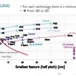
Arnaud Furnemont’s talk was titled “From Technology Scaling to System Optimization”. Simple 2D … Read More