For 20 years PDF Solutions have been working with fabs on yield enhancement. Today, they announced their Exensio Platform for big data manufacturing environments. They haven’t really been keeping it a secret and have been talking about it at events since late last year, but it has basically been in stealth mode for the last… Read More

Tag: yield
Coventor Panel at IEDM Digs into Variation Issues
Recently I attended a panel discussion on variability in semiconductor fabrication hosted by Coventor in conjunction with the IEEE IEDM conference in San Francisco. The IEEE bills the conference as “the world’s pre-eminent forum for reporting technological breakthroughs in the areas of semiconductor and electronic device… Read More
In-Design DFM Signoff for 14nm FinFET Designs
While FinFET yield controversy is going on, I see a lot being done to improve that yield by various means. One prime trend today, it must be, it’s worthwhile, is to pull up various signoffs as early as possible during the design cycle. And DFM signoff is a must with respect to yield of fabrication. This reminds me about my patents filed… Read More
Semiconductor Fabrication Module Optimization

The growing process integration complexity at each technology node has increased development time and cost, and this trend looks to continue. There is a looming risk of delivering unrepeatable critical unit processes (or process modules) that would require revisiting development and manufacturing requalification or in … Read More
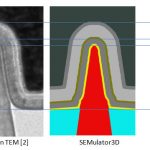
Rapid Yield Optimization at 22nm Through Virtual Fab

Remember? During DAC2013 I talked about a new kind of innovation: A Virtual Fabrication Platform, SEMulator3D, developed by COVENTOR. Now, to my pleasant surprise, there is something to report on the proven results from this platform. IBM, in association with COVENTOR, has successfully implemented a 3D Virtual Fabrication… Read More
A Goldmine of Tester Data
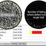
Yesterday at SEMICON West I attended an interesting talk about how to use the masses of die test data to improve silicon yield. The speaker was Dr. Martin Keim, from Mentor Graphics.
First of all, he pointed out that with advanced process nodes (45nm, 32nm, and 28nm), and new technologies like FinFETs, we get design-sensitive defects.… Read More
Yield Analysis and Diagnosis Webinar
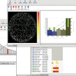
Sign up for a free webinar on December 11 on Accelerating Yield and Failure Analysis with Diagnosis.
The one hour presentation will be delivered via webcast by Geir Eide, Mentor’s foremost expert in yield learning. He will cover scan diagnosis, a software-based technique, that effectively identifies defects in digital logic… Read More