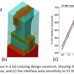
For any semiconductor technology node to be adopted in actual semiconductor designs, the very first step is to have a Process Design Kit (PDK) developed for that particular technology node and qualified through several design tools used in the design flow. The development of PDK has not been easy; it’s a tedious, time consuming,… Read More
Tag: virtual metrology
SEMulator3D 2014 – New Enhancements for Virtual Fabrication in the 3D IC Era
A Virtual Platform for any kind of design or manufacturing in any discipline of science or engineering (electrical, mechanical, aeronautics etc.) must be able to provide an accurate representation of an actual design/product in a fraction of time and cost it takes to build working prototypes. In the case of semiconductors at … Read More
Semiconductor Fabrication Module Optimization
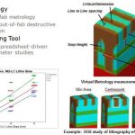
The growing process integration complexity at each technology node has increased development time and cost, and this trend looks to continue. There is a looming risk of delivering unrepeatable critical unit processes (or process modules) that would require revisiting development and manufacturing requalification or in … Read More
What Can Accelerate 3D Semiconductor Manufacturing?
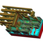
In the beginning of this decade there was a lot of buzz around 3D chip manufacturing. Many EDA tools were developed to facilitate semiconductor designs in 3D space. Naturally, we are moving to the edge on 2D without much room to further squeeze transistors and interconnect. However, lately I haven’t heard much about 3D products.… Read More
How to Quickly Optimize BEOL Process at Your Desk?
Engineers are always looking to improve the efficiency of how they work, but don’t want to sacrifice accuracy in the process. This is true in the world of semiconductor process development, where traditional build-and-test cycles are both time and resource intensive. But what if there was a way to do certain steps in a ‘virtual’… Read More


