Featured Speakers:
- Jerome Toublanc, Product Management, Principal, Synopsys
As advanced-node and multi-die designs push power delivery networks to their limits, accurately understanding voltage behavior has become essential for both signoff confidence and design optimization. Traditional approaches often struggle… Read More
Synopsys is catalyzing the era of pervasive intelligence with comprehensive engineering solutions spanning silicon design, IP, and simulation and analysis. At this year’s Design Automation Conference (DAC), the company will showcase innovations transforming silicon and systems development for a wide range of applications… Read More
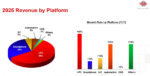
The semiconductor landscape is currently undergoing a structural transformation as the “Data-Centric Shift” moves the industry’s center of gravity from smartphones toward High-Performance Computing (HPC) and AI infrastructure.
This transition is clearly validated by TSMC’s 2025 filings, which show… Read More
Webinar Overview:
Is formal verification ready for general use or do you need a PhD to use it? Larger companies continue to recruit formal PhDs into their verification teams while other less-well-qualified engineers seem reluctant to go beyond simplified formal “apps”.
So, what is the truth of the matter? Can non-specialist… Read More
In the early 1980s, when computer-aided engineering (CAE), the precursor to modern electronic design automation (EDA), was just taking shape, my professional trajectory shifted in a way that would prove foundational. I joined Teradyne, the Boston-based leader in automated test equipment (ATE), and I encountered for the first… Read More
Synopsys Foundation IP for Intel 18A is a portfolio of semiconductor building blocks designed to help system-on-chip developers build advanced chips with better power, performance, and area, often called PPA. The offering includes embedded memory compilers, standard-cell logic libraries, and input/output libraries for… Read More
Featured Speaker:
- Manmeet Walia, Executive Director of Product Management, Synopsys
AI performance is no longer limited by compute—it’s limited by how efficiently data moves. As systems scale to compute-dense clusters, memory, die-to-die, and high-speed interfaces are emerging as critical bottlenecks.
This webinar explores… Read More
Featured Speakers:
- Richard Solomon, Senior Staff Technical Product Manager, Synopsys
- Ron Lowman, Staff Product Manager, Synopsys
Heterogeneous compute platforms are driving new requirements for connectivity across increasingly complex system architectures. This webinar explores how PCIe and CXL can be used to provide… Read More
For the past decade, the semiconductor industry has been moving in one direction: shift-left, specifically, shifting more validation into the pre-silicon phase. The idea was straightforward: if software ultimately determines how a system behaves, then software should become a primary vehicle for verification.
The industry… Read More