You are currently viewing SemiWiki as a guest which gives you limited access to the site. To view blog comments and experience other SemiWiki features you must be a registered member. Registration is fast, simple, and absolutely free so please,
join our community today!
As you know, I’ve been a bit of a bear about what is happening to wafer costs at 20nm and below. At the Common Platform Technology Forum last week there were a number of people talking about this in presentations and at Harvey Jones’s “fireside chat”.
At the press lunch I asked about this. There are obviously… Read More
In July Cadence acquired Sigrity, one of the leaders in PCB and IC packaging analysis. Until a decade ago, signal integrity and power analysis was something that only IC designers needed to worry about. For all except the highest performance boards, relatively simple tools were sufficient. Provided you hooked up the pins on all… Read More
9 Micron Wooden Gateby Paul McLellan on 02-08-2013 at 4:55 pmCategories: General
When I started in this business, we were at 3 micron HMOS. A few other things are close to that size. A red blood cells is about 9 microns, a human hair is about 100 microns. And in a bizarre “only in Japan” video, people compete to plane the thinnest shaving off a plank of wood. It turns out the answer is 9 microns. That’s… Read More
The numbers are starting to come in for how everyone did in Q4. According to Cannacord Genuity, Apple made 69% of the profit and Samsung made 34%. What do you notice about those numbers? They add up to more than 100%. HTC supposedly made 1% of the profit and everyone else either broke even or lost money. Basically Apple and Samsung have… Read More
Tubes of the Futureby Paul McLellan on 02-07-2013 at 10:00 pmCategories: General
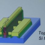
So what is a silicon nanowire? It is basically a FET where the active element is a wire 3-20nm in diameter. So where a FinFET has the gate wrapped around 3 sides of the transistor, a nanowire (NW) has it wrapped around all four. In essence, the wire runs through the middle of the gate.
There seem to be three issues about building a silicon… Read More
The most interesting session at the Linley Tech Data Center Conference last week was the last one, on Designing Power Efficient Servers. What this was really about was whether ARM would have any success in the server market and what Intel’s response might be.
Datacenters are now very focused on power efficiency and many track… Read More
I was at the Common Platform Technology Forum this week. One of the most interesting sessions is IBM’s Gary Patton giving an overview of the state of semiconductor fabrication. Then, at lunchtime, he is one of the people that the press can question. In this post, I’m going to focus on Extreme Ultra-Violet (EUV) lithography.… Read More
Calypto announced that Sanjiv Kaul is the new CEO. I first met Sanjiv many years ago when he was still at Synopsys when I interviewed for a position there around the time I transitioned out of Compass and went back to the parent company VLSI. I forget what the position was. Then about three or four years ago when I did some work for Oasys… Read More
Power is a fundamentally hard problem. When you have finished the design, you have accurate power numbers but can’t do anything about them. At the RTL level you have some power information but it is often too late to make major architectural changes (add an offload audio-processor, for example). Early in the design, making… Read More
What is the biggest challenge facing an EDA startup today? By a startup, I mean a brand new company, not a company that already has a few customers and is either on a fast path to success or a slower path whereby the company can continue to grow slowly forever.
Obviously, one challenge is the funding environment. Since EDA acquisitions… Read More