You are currently viewing SemiWiki as a guest which gives you limited access to the site. To view blog comments and experience other SemiWiki features you must be a registered member. Registration is fast, simple, and absolutely free so please,
join our community today!
By Todd Burkholder and Per Viklund, Siemens EDA
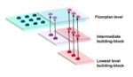
The landscape of advanced IC packaging is rapidly evolving, driven by the imperative to support innovation on increasingly complex and high-capacity products. The broad industry trend toward heterogeneous integration of diverse die and chiplets into advanced semiconductor… Read More
My first exposure to seeing multiple die inside of a single package in order to get greater storage was way back in 1978 at Intel, when they combined two 4K bit DRAM die in one package, creating an 8K DRAM chip, called the 2109. Even Apple used two 16K bit DRAM chips from Mostek to form a 32K bit DRAM, included in the Apple III computer, circa… Read More